In 2020, global energy consumption grew to over 173000 terawatt-hours, which is more than 30 times the world’s energy consumption at the beginning of the industrial revolution.1,2
Global energy consumption is predicted to double by 2100, meaning the development of sustainable energy generation technologies is growing ever more urgent.
Currently, approximately 10% of the total energy consumption is supplied by modern renewables, with solar power accounting for just 1% of this. Though it presently generates a small percentage of the global energy needs, solar power offers great promise to take a greater share in the future.
Photovoltaic technology, which directly converts sunlight into electricity, has the potential to take advantage of this massive renewable energy resource.
Silicon was the first photovoltaic material and was used to power space missions in the 1950s. The recent expansion in solar cell research has been motivated by the requirement to improve renewables’ share in the overall global energy mix.
A growing area of research has focused on organic photovoltaics (OPVs), spurred on by breakthroughs in the 1980s that saw their current densities surpass the mA/cm2 range and attain 1% photoconversion efficiency (PCE).3,4
Since then, current densities have reached >20 mA/cm2, making them comparable to inorganic photovoltaics. Their PCEs have also progressively increased to >18%, making organic photovoltaics a commercially viable source of energy.
OPVs offer greener manufacturing technologies over their conventional photovoltaic counterparts.5 The carbon-based raw materials from which OPVs are manufactured are abundant, inexpensive, and non-toxic.
Because OPVs can be applied via solution processing or vacuum coating, manufacturing processes can be easily and economically scaled up for commercial production.
OPVs also offer compatibility with flexible substrates that are suitable for roll-to-roll production of lightweight devices. This opens up the possibility for OPVs to be used in new applications, such as building-integrated photovoltaics (BIPVs).
These benefits, in aggregate, suggest that OPVs can be produced at lower cost than existing PV technologies and thus deployed more easily and broadly to increase the use of renewable energy on a global scale.
Inside a solar cell is a material with light-absorbing properties that forms excitons when illuminated. These subsequently split into positive and negative charge carriers.
Organics usually form excitons that are tightly bound and possess limited diffusion lengths - owing to their lower permittivity in comparison to inorganic materials – leading to a greater probability of recombination and lower PCEs.4
To combat this inherent limitation, OPVs can be sensitized by combining various donor and acceptor molecules that promote charge transfer between them. Charge formation can only occur at the donor-acceptor heterojunction, a point where the diffusion length is approximately 10 nm.
Blended junctions - versus two-layer junctions - are applied via co-deposition of the donor and acceptor materials to maximize their interface. Donor-acceptor sensitization can happen within bulk heterojunctions (BHJs), which then behave like an intrinsic semiconductor.
Substantial opportunities exist for improving the PCE of OPVs by fully enhancing the structure of bulk heterojunctions (Figure 1A). For example, phase separation is vital in the formation of the distributed donor-acceptor interface where excitons are produced within the diffusion length of the heterojunction.5
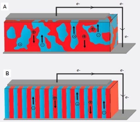
Figure 1. (A) Bulk heterojunction morphology versus (B) vertically aligned block copolymer morphology. Image Credit: Asylum Research - An Oxford Instruments Company
When formed, the electrons and holes can only move within acceptor and donor molecules, respectively. Charge extraction therefore requires a percolation network - formed from donor and acceptor phases - that provides routes for charge transport to the electrodes.
The engineering of the BHJ microstructure is accomplished by means of controlling the self-assembly of their components into well-defined phases - a vital element in improving their PCEs.
Atomic force microscopes (AFMs) can resolve the microscopic phase structure of OPVs down to the scale of the heterojunction diffusion length.
AFMs can easily capture surface topography at the nanometer scale to reveal how variables like roughness and morphology can impact performance during processing.
AFM probes make physical contact with the surface, facilitating the concurrent measurement of surface topography with other material properties, for example, conductivity or surface potential.
Short-circuit current and open-circuit voltage - which can have a direct impact on PCEs - can be calculated thanks to the AFMs’ high spatial resolution, resulting in unique and detailed data that assists in OPV engineering.6
This article focuses on recent publications that establish how Oxford Instruments Asylum Research AFMs can be used to resolve the microstructure of OPVs, leading to improvements in their processing and performance.
Evaluating Phase Segregation of Block Copolymer OPVs with Tapping Mode Phase Imaging to Improve Charge Generation
Among the most well-studied OPV systems is the poly(3-hexylthiophene) (P3HT) and [6,6]-phenyl C61- butyric acid methyl ester (PCBM) donor-acceptor pair. When blended, they form a bulk heterojunction (Figure 1A).
The high interfacial area between the donor and acceptor phases improves charge generation. Their network arrangement within the bulk heterojunction creates percolation pathways for charge transport and collection.
While their processing is normally straightforward, the requirements for mixing, spin-coating, and annealing processes, must be adjusted to increase the donor-acceptor interfacial area and percolation network.
By allowing users to visualize the surface morphology and quantify the roughness of OPV thin films, AFMs can be utilized in phase structure analysis, providing critical data for optimizing processing steps.
One option for controlling the spatial arrangement of donor and acceptor components is combining both into block copolymers. These are known to self-assemble into ordered morphologies, with domain sizes determined by polymer flexibility and chain length.7
BHJs remain metastable structures (even after annealing), kinetically frozen above their thermodynamic minimum, which allows them to phase separate over time into coarser domains, leading to poor aging performance.
Block copolymers can form stable lamellar structures, which, if oriented perpendicular to the electrodes (Figure 1B), can potentially offer both a maximal donor-acceptor interface and direct percolation paths for charge collection.
Researchers at the University of Melbourne have synthesized an OPV block copolymer by covalently linking the P3HT acceptor molecules with PFTEGT6BT donor molecules.7
Tetraethylene glycol sidechains were adhered to the donor molecule to improve phase segregation.
Researchers compared the performance and structure of thin films made from this copolymer to thin films formed by phase separation, conventional blending, and annealing of the homopolymers.
Figure 2A shows tapping mode phase images of a blend of the homopolymers P3HT and PFTEGT6BT that were spin-coated into a thin film which was then annealed at 200 °C for 1 hour and 45 minutes.
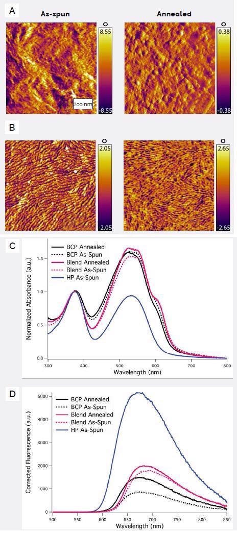
Figure 2. Tapping mode phase images of films of (A) PFTEGT6BT/P3HT blend, and (B) P3HT-b-PFTEGT6BT deposited from 2 wt % 4-bromoanisole in o-xylene before and after annealing. (C) UV/vis absorption spectra of films P3HT-b-PFTEGT6BT block copolymer (BCP), PFTEGT6BT (“HP”), and P3HT/PFTEGT6BT (“Blend”) normalized to absorption at 370 nm. (D) Fluorescence spectra of the same films, excited at 370 nm and adjusted for differences in absorption at that wavelength. Note: PFTEGT6BT= poly(2,7-(9,9′-dioctylfluorene)-alt-5,5-(4′,7′-dithienyl-2′,1′,3′-benzothiadiazole with tetraethylene glycol side-chains affixed to the fluorenyl unit. Image Credit: Asylum Research - An Oxford Instruments Company
The homopolymers’ composition in the resulting blend matched that of the block copolymer when compared. The as-spun film was mainly featureless other than dense areas of rod-like structures that P3HT is known to form.
Post-annealing, the surface was noticeably smoother, conceivably due to the preferential segregation of the comparatively amorphous PFTEGT6BT component on the surface.
A very distinctive formation of linear domains is observable in the thin films formed from the P3HT-b-PFTEGT6BT block copolymer, a feature that becomes sharper and more distinct with annealing (Figure 2B).
This rod-like polymer’s contour length was calculated to be 44-50 nm, based on the molecular weight obtained via gel permeation chromatography. The domain sizes were predicted to be 22-25 nm in length, a range consistent with the 20 nm domains seen in the AFM images.
Tapping mode phase imaging is a powerful method to visualize polymer blends. The phase signal will vary as a function of contact area, stiffness, adhesion, and viscous losses. These will change the tip-sample interaction, depending on the component of the material being probed.
Asylum Research AFMs’ ultra-low noise electronics allow for phase imaging with very high sensitivity. This enables phase imaging to precisely resolve domains in polymer blends, even in cases where they are not clear when viewed in topographic images.
Though the image contrast is qualitative in nature, phase imaging frequently yields higher levels of resolution when compared to fast force-curve modulus mapping. The latter requires significant indentation into the surface and consequently a larger tip-sample contact area.
The charge transfer between donor and acceptor moieties can be seen clearly from the quenching of photoluminescent intensity (Figure 2C and Figure 2D). Larger amounts of quenching were seen in the block copolymer (85% as-spun and 74% after annealing) in comparison to the blend (69% as-spun and 66% after annealing).
This suggests superior morphological control and inhibition of macrophase separation provided by covalent linking of the two groups - something revealed in the AFM data.
AFM was vital in validating the anticipated phase separation of donor and acceptor moieties in instances where they are prepared as block copolymers, in contrast to a blend of homopolymers, resulting in more efficent charge transfer performance.
Though there were greater efficiencies in charge generation, this OPV system largely displayed a low PCE. It is possible that the tetraethylene glycol sidechains that were added to enhance phase segregation impeded electron mobility and restricted charge transport efficiency.
Another approach is to utilize a compatibilizing molecule to accurately control phase segregation throughout melt processing.
Evaluating Melt Processing of Small Molecule OPVs with Kelvin Probe Force Microscopy (KPFM) to Improve Photoconversion Efficiency
Solution processing is among the most extensively researched approaches to OPV fabrication as it presents many opportunities for engineering bulk heterojunctions, allowing for better performance and lower cost. These methods can also be adapted to accommodate scaled-up roll-to-roll manufacturing methods.
However, the chlorinated or aromatic solvents needed are toxic in nature, which reduces the ‘green’ benefits attributed to OPVs.
Less toxic or more benign solvents frequently involve altering the OPVs’ molecular structure to enhance solubility or dispersion in colloidal systems. Either of these options can affect their final solid-state form and optoelectronic properties.
Researchers at EPFL in Lausanne studied solvent-free manufacturing of OPVs via melt processing from a solid dispersion, utilizing a molecular compatibilizer (MCP) additive to manage the phase segregation.8
The molecular structures of the small donor and acceptor molecules, DPP(TBFu)2 and EP-PDI, along with the compatibilizing additive molecule - effectively the same donor and acceptor molecules which are linked by a short (non-conjugated) aliphatic chain that preserves their individual π-conjugated structures - are shown in Figure 3A.
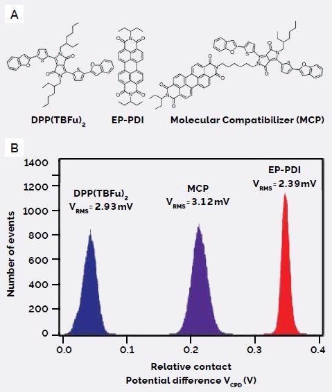
Figure 3. (A) Molecular structures of the donor, DPP(TBFu)2, acceptor, ED-PDI, and molecular compatibilizer, MCP, and (B) their corresponding relative contact potential differences (VCPD), measured by KPFM. Image Credit: Asylum Research - An Oxford Instruments Company
Both DPP(TBFu)2 and EP-PDI are highly crystalline solids, shown by the sharp melting transitions in their differential scanning calorimetry (DSC) curves. MCP does not display any transition, signifying its amorphous nature.
In melt processing, a 1:1 solid dispersion of donor and acceptor materials is heated in excess of the melting temperature to a single-phase liquid melt. It is then allowed to solidify in the presence of a compatibilizing additive that controls the phase segregation of the BHJ.
Liquefaction and annealing were achieved at 240 °C, which is above the melting temperature of DPP(TBFu)2 (Tm = 231 °C). This contrasts with solution processing where the BHJ film is thermally annealed at temperatures below the melting point.
The systematic addition of MCP causes the melting transition peaks in DSC curves to diminish and shift to lower temperatures. This is expected of a compatibilizer as it disturbs the crystal structures of the separate elements.
Crystallinity was also tracked via XRD and indicated only a residual ordering of the donor component at 50 wt% MCP. There was considerable ordering of the acceptor component even at 75% wt% MCP.
AFM can directly visualize the nanoscale morphology of these preparations of BHJs with different MCP loading.
Topographic images of a range of melt-processed BHJs with 0-100 wt% MCP show noticeable differences (Figure 4A).
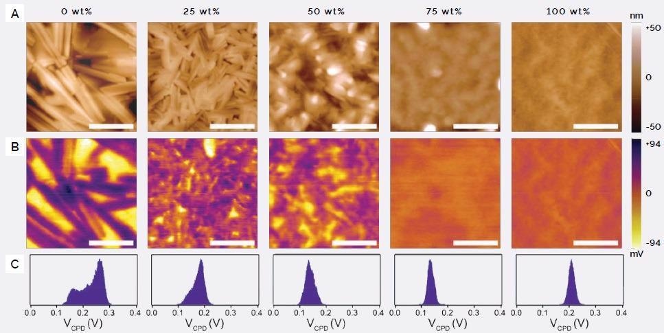
Figure 4. (A) Topographic images of melt-annealed (240°C) BHJ thin films of DPP(TBFu)2:EP-PDI (1:1 by weight) with varying amounts of MCP, with 100% being pure MCP; (B) corresponding KPFM surface potential images, measured under dark ambient conditions; (C) histograms of contact potential difference (VCPD) for each KPFM image. Image Credit: Asylum Research - An Oxford Instruments Company
In the absence of MCP, large, rod-like crystallite domains form that are hundreds of nanometers in length. These reduce in size with the addition of up to 50 wt% MCP. At 75 wt% the film appears virtually homogenous and is similar to the morphology of pure MCP.
The surface potential of materials at the nanoscale level can be mapped using Kelvin Probe Force Microscopy (KPFM).
Phase segregation can be revealed by KPFM as the constituent materials are distinguishable by their contact potential difference (VCPD) with the Pt AFM tip.
In this study, KPFM was used on an Asylum Research Cypher AFM that can readily resolve sub-mV potential variations.
DPP(TBFu)2 has a lower VCPD compared to EP-PDI, which is expected between donor and acceptor molecules, while the MCP was shown to have an intermediate VCPD value (Figure 3B).
From this, the chemical nature of the phase domains in the series of KPFM images of melt-processed BHJs at different MCP loading can be interpreted (Figure 4B).
At 0 wt% MCP, the donor and acceptor components are clearly phase segregated into the following:
- Large platelet-shaped DPP(TBFu)2 crystals (in yellow)
- Rod-like EP-PDI crystals (in purple)
The extent of the segregation is likewise suggested by the bimodal shape of the VCPD histogram (Figure 4C).
As increasing amounts of MCP are added, the KPFM images indicate the donor and acceptor domains reduce in size, and donor-acceptor mixing increases as indicated by the VCPD histogram becoming more narrow and unimodal.
At 75 wt% MCP, the surface potential is virtually homogeneous and comparable to pure MCP. The AFM data indicates that the quality of the phase segregation of donor and acceptor components in melt-processed BHJs can be fine-tuned to a high degree via a compatibilizing additive.
MCP loading and the quality of phase segregation can affect indicators of device performance (Figure 5). For example, photoluminescence quenching (PLQ) increased, while the relative molecular ordering (RMO) decreased as the MCP loading increased and the BHJ became more homogenous.
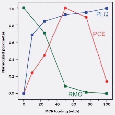
Figure 5. Effect of MCP on DPP(TBFu)2:EP-PDI BHJ morphology and device performance, shown with normalized parameters: photoconversion efficiency (PCE), photoluminescence quenching (PLQ, from PL emission data), and relative molecular ordering (RMO, from XRD scattering data). Image Credit: Asylum Research - An Oxford Instruments Company
PLQ is a sign of charge generation, occurring at the heterojunction, and is favored by an increased donor-acceptor interface at higher MCO loading.
RMO suggests the presence of suitably sized pure domains that are large enough to allow the creation of a percolation network for efficient charge transport to the electrodes.
The peak in PCE at 50 wt% MCP indicates that there is a correlation between the two effects. Charge generation only slightly rises as the BHJ becomes more homogeneous beyond 50 wt% MCP.
This is at the cost of declining charge transport and collection efficiencies due to a dearth of pure donor and acceptor domains to create a percolation network.
Evaluating Substrate Ozonation to Increase Wetting of Aqueous OPV Nanoparticle Inks in Roll-to-Roll Manufacturing of Solar Cell Devices
OPV research often focuses on enhancing the PCE of the photo-absorbing material to levels that are close to those of solar technologies already available on the market. This normally involves optimizing the processing of BHJs into well-defined microphases that promote charge generation, transport, and collection.
While commercialization is important, so is the suitability of production methods to upscaled device fabrication. Roll-to-roll manufacturing is particularly promising in this regard.
This method involves a roll of flexible substrate being coated or printed with layers of active materials in series and subsequently spun back to an output roll. The process is presently utilized in the production of flexible OLED devices and is also being developed for flexible OPVs.
The photo-absorbing material, metal electrodes, and charge transport layers are all applied like ink on flexible substrates via a number of methods, including:
- Screen printing
- Slot-die coating
- Flexographic printing
Researchers from Iraq and Australia have examined the suitability and technical hurdles of employing organic photo-absorbers in this manner.9
The utilization of toxic and/or hazardous solvents required to dissolve these organic materials remains a concern.
The use of water and the greener organic solvents, for example, alcohols, frequently required modification of the structure of these largely hydrophobic molecules to enhance their solubility. This may affect their phase segregation and optoelectronic properties.
The groups’ methodology involved formulating these organic electronic materials into emulsions by utilizing surfactants to disperse them in water. This meant they could be used in roll-to-roll production as aqueous solar nanoparticle (ASNP) inks.
The application of solar materials in the form of inks inevitably entails that they wet the substrate, which in this instance is typically poly(3,4-ethylenedioxythiophene):poly(styrene sulfonate) (PEDOT:PSS) - a flexible plastic material that is transparent and conductive in terms of hole transport.
One process for engineering the surface energy to ensure satisfactory wetting is by controlling the amount of excess surfactant in the ASNP.
Previous research showed that inks encapsulated in sodium dodecyl sulfate (SDS) surfactants led to optimal wetting performance at SDS concentrations where the surface tension was around 48 mN/m.
While free surfactant concentration assists in the formation of a film, it may also have a negative impact on the overall performance of the device, considering the low PCEs that were found.
Another option is to enhance the wettability of the substrate by subjecting it to UV-ozone exposure. This leads to the creation of carboxyl and hydroxyl groups on the organic surface that can assist in the wetting of aqueous-based inks.
To optimize the exposure time, treated substrates were visualized with AFM to assess surface roughness and subsequent ASNP film quality.
These experiments were carried out on an Asylum Research Cypher AFM, which features industry-leading low-noise imaging performance with a noise floor of just 15 pm (half that of any other commercial AFM). This allowed the precise measurement of film roughness variations at sub-Angstrom levels.
PEDOT:PSS-type substrates following 0 to 30 minutes of exposure to UV- ozone and subsequently spin-coated with ASNP films were scanned at 5 µm (Figure 6). The UV-ozone treatment of the substrate caused a minor rise in surface roughness, though the morphology remained the same up to 15 minutes of exposure.
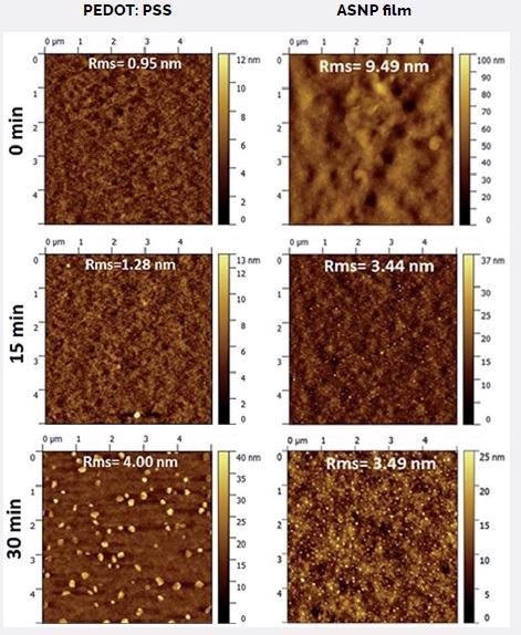
Figure 6. Topographic images of PEDOT:PSS-type substrates after 0 to 30 min exposure to UV-ozone, and the corresponding ASNP film spin-coated on the substrate after treatment. Image Credit: Asylum Research - An Oxford Instruments Company
Following a 20 minute exposure (not displayed), small aggregates (≤100 nm) were observed, which increased in volume and quantity following a 30 minute exposure.
The contact angle rapidly dropped from 16° to 3° after 5 minutes of exposure. The work function - measured by photoelectron spectroscopy in air - substantially increased after 20 minutes of exposure.
Such findings indicate that the necessary wettability is conferred to the PEDOT:PSS surface within 5 minutes of UV-ozone exposure, with no significant changes in the morphology of the surface.
The substrate treatments outlined above depend on the nature of the ASNP films produced by spin-coating. Topographic images of the matching ASNP films indicate large pinholes and surface asperities on films cast on untreated substrates (Figure 6).
Films prepared on substrates that were UV-ozone-treated for at least 5 minutes were significantly smoother, with a strong (~43%) reduction in roughness. The film morphology did not alter significantly with greater exposure times on this substrate.
Other kinds of PEDOT:PSS substrates (not displayed) used in higher conductivity applications exhibited higher roughness and formation of larger aggregates after longer exposures.
These results show shows how AFM can be utilized to assess ASNP film quality after the substrate has been treated for improved wettability.
Summary
Organic photovoltaics have the potential to become a very low-cost source of energy when it comes to ease of processing, material cost, and scalability of manufacturing.
In order to compete with inorganic technologies already on the market, the photoconversion efficiencies and device lifetimes of OPVs require improvement, and the environmental impact of their manufacture must be reduced.
By nature, OPVs require sensitization by intimately mixing donor and acceptor components into bulk heterojunctions, where PCEs are extremely dependent on the microstructure.
This necessitates the need to employ optimization during the production process to maximize results in areas like charge generation, transport, and collection.
This article explored how AFM topographic imaging, phase imaging, and surface potential mapping could assist with engineering optimal phase segregation within BHJs of melt-processed small molecule OPVs and solution-processed block copolymer OPVs.
Besides assisting in the manufacture of more efficient photoabsorbers, AFMs can also be utilized in engineering surface energies to optimize the use of water-based OPVs on flexible substrates in roll-to-roll manufacturing.
This demonstrates the critical roles AFMs can play in all aspects of OPV development, from basic research right through to process engineering, development, and scalable manufacturing.
References
- Our World in Data, “Global primary energy consumption by source” (https://ourworldindata.org/energy-production-consumption)
- Looney, B. “Statistical Review of World Energy, 2020.” (2020).
- NREL, “Best Research-Cell Efficiency Chart” (https://www.nrel.gov/pv/cell-efficiency.html)
- Hiramoto, Masahiro, and Yusuke Shinmura. “Organic Solar Cells.” In Springer Handbook of Electronic and Photonic Materials, pp. 1-1. Springer, Cham, 2017.
- Riede, Moritz, Donato Spoltore, and Karl Leo. “Organic Solar Cells—The Path to Commercial Success.” Advanced Energy Materials 11, no. 1 (2021): 2002653.
- Atamanuk, Katherine, Justin Luria, and Bryan D. Huey. “Direct AFM-based nanoscale mapping and tomography of open-circuit voltages for photovoltaics.” Beilstein journal of nanotechnology 9, no. 1 (2018): 1802-1808.
- Mitchell, Valerie D., Eliot Gann, Sven Huettner, Chetan R. Singh, Jegadesan Subbiah, Lars Thomsen, Christopher R. McNeill, Mukundan Thelakkat, and David J. Jones. “Morphological and device evaluation of an amphiphilic block copolymer for organic photovoltaic applications.” Macromolecules 50, no. 13 (2017): 4942-4951.
- Rahmanudin, Aiman, Liang Yao, Xavier A. Jeanbourquin, Yongpeng Liu, Arvindh Sekar, Emilie Ripaud, and Kevin Sivula. “Melt-processing of small molecule organic photovoltaics via bulk heterojunction compatibilization.” Green Chemistry 20, no. 10 (2018): 2218-2224.
- Almyahi, Furqan, Thomas R. Andersen, Adam Fahy, Michael Dickinson, Krishna Feron, Warwick J. Belcher, and Paul C. Dastoor. “The role of surface energy control in organic photovoltaics based on solar paints.” Journal of Materials Chemistry A 7, no. 15 (2019): 9202-9214.

This information has been sourced, reviewed and adapted from materials provided by Asylum Research - An Oxford Instruments Company.
For more information on this source, please visit Asylum Research - An Oxford Instruments Company.