Sponsored by Nanosurf AGReviewed by Olivia FrostJan 6 2023
Kelvin probe force microscopy (KPFM) belongs to a suite of electrical characterization methods made available in scanning probe microscopes. It maps the contact potential difference (CPD) between a surface and the cantilever, including information relative to the surface potential and work function.
According to solid-state physics, the work function is categorized as the energy required to remove an electron from the Fermi level of a solid to the vacuum and, therefore, is a surface property. It is not affiliated with the bulk. Accordingly, KPFM is a surface-sensitive method that only probes at and near the surface. It is generally used as a qualitative technique to acquire contrast based on the surface potential.
Quantitative KPFM measurements of the local work function are usually performed in a vacuum and necessitate a model to detail the electrostatic interactions occurring between the tip and sample as well as understanding the work function of the tip.
In ambient conditions, surface contaminations of the tip and sample can influence the contact potential difference. Furthermore, surface water films can also influence the CPD, which hampers the calculation of the work function of a sample surface.
How Does it Work?
On Nanosurf AFMs, Kelvin probe force microscopy functions in dynamic force mode, where a cantilever with a thin electrically conductive coating is driven close to its resonance frequency. Soft dynamic mode cantilevers coated with platinum-iridium (PtIr) are well-suited to be used in most KPFM experiments and are not much more expensive than their non-conductive variants. Otherwise, cantilevers coated with conductive diamond-like carbon or Platinum silicide are available and have increased wear resistance compared to PtIr.
An AC voltage, with frequency placed at a distance from the resonance frequency, is applied to the cantilever to measure the CPD between the surface and the cantilever. This generates an oscillating electrostatic force between the tip and sample that can be measured by a second internal lock-in amplifier in the controller, as displayed in Figure 1.
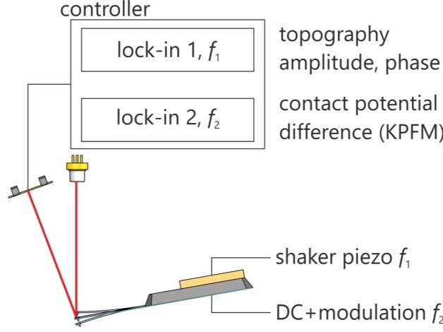
Figure 1. Schematic of KPFM. Image Credit: Nanosurf AG
A DC offset voltage is then introduced to the AC voltage to offset the cantilever oscillation at the AC frequency. By recording the DC offset voltage applied while the tip is scanned across the surface, a representation of the CPD appears. An intuitive KPFM routine in the Nanosurf software makes configuring KPFM measurements relatively easy, allowing even novice users to acquire KPFM data. KPFM has functionality in both single and dual-pass modes. In single-pass mode, the cantilever moves across every line once while simultaneously recording topography and CPD.
The benefit of using single-pass mode is that the simultaneous recording of the topography and CPD enhances the correlation between the signals. If the cantilever oscillation amplitude remains small, the tip is close to the surface, which increases the sensitivity and resolution of the KPFM measurement. Single pass KPFM minimizes tip wear and is also faster but is more vulnerable to artifacts at edges and boundaries.
In the dual-pass setup, the cantilever passes over each line in the image twice. The topography information is collected during the first pass. The tip is then adjusted or lifted above the sample during the second pass by a user-determined distance, generally somewhere in the region of just a few tens of nanometers.
The CPD is recorded as described above. Dual-dual pass measurements are essentially slower than single-pass measurements because each line must be imaged twice. Ideally, the topography recorded during the first pass is used during the second pass to ensure constant tip-sample separation.
While longer acquisition times are required when compared to the single-pass method, the main advantage is fewer edge and boundary artifacts and less noisier images. By reducing the oscillation of the cantilever during the second pass, reduction of the lift height is possible, enhancing the KPFM contrast.
KPFM Applications
A. Multilayer Graphene: Multilayer graphene can exhibit a range of novel electrical properties depending on composition. An 8 x 8µm image at the edge of a graphene flake is displayed in Figure 2. The sample is a multilayer graphene flake produced by mechanical exfoliation of graphite and subsequently transferred to a silicon-silicon dioxide substrate. (Sample supplied by Hiske Overweg and Klaus Ensslin, ETH Zürich, Switzerland).
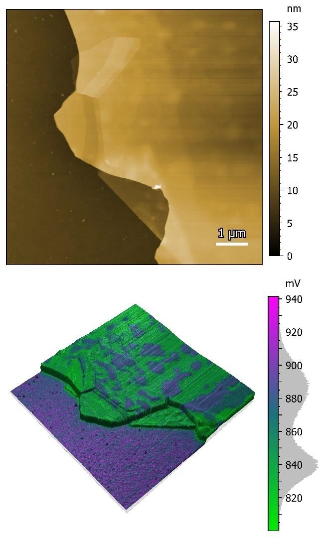
Figure 2. Multilayer graphene. The top image is an 8 x 8 μm topography image while the bottom image shows the 3D representation of the surface topography overlaid with the contact potential difference. Sample courtesy of Hiske Overweg and Klaus Ensslin, ETH Zürich, Switzerland. Image Credit: Nanosurf AG
The top image shows the topographical map, while the bottom image displays the KPFM signal superimposed onto a 3D representation of the surface topography. The color contrast in this map depicts the KPFM signal or the contact potential difference.
Areas shown purple or pink indicate those with high contact potential difference, while green areas possess low contact potential difference. Through this CPD map, the electrical properties at various flake thicknesses are evident as the thin flakes on top possess a high contact potential (blue). At the same time, the rest of the layer has a lower contact potential (green).
B. MoS2 Monolayer: Another example of KPFM’s power, particularly as a method to deliver electrical properties contrast, is demonstrated in the study of a molybdenum disulfide (MoS2) monolayer, grown by chemical vapor deposition (CVD).
Utilizing the Flex-Axiom, KPFM shows the contact potential difference variations across a single crystal as well as variations between the single crystal and the SiO2 substrate. An 18 x 18 µm image of the monolayer is displayed in figure 3.
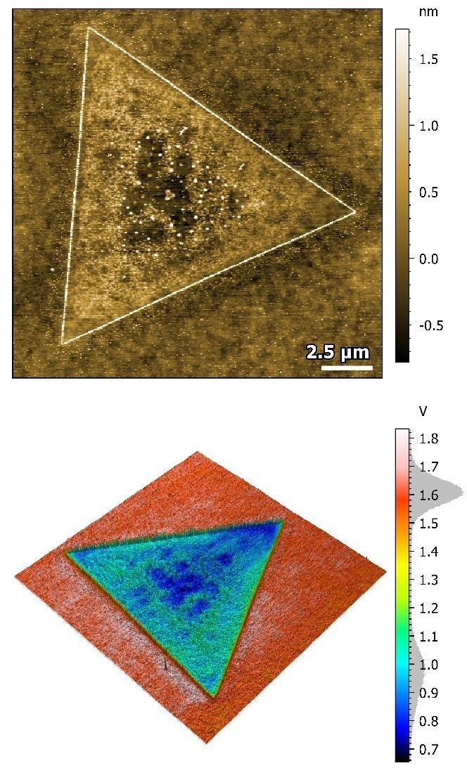
Figure 3. MoS2 Monolayer. The top image is an 18 x 18 μm topography image while the bottom image shows the 3D representation of the surface topography overlaid with KPFM signal. Image Credit: Nanosurf AG
The top image is the topography, while the bottom image represents the KPFM signal superimposed on a 3D representation of the surface topography. There is a 650 mV contact potential difference between the monolayer and the substrate, even though the monolayer is only 0.6 nm thick. The contact potential signal fluctuates across the monolayer, supplying relevant information regarding doping profiles and other surface defects.
C. KPFM on Steel: Stainless steel is a metal alloy made up of elements such as chromium, aluminum, and carbon, and bound in a ferrite matrix. The work potential of each element that make up the steel will vary slightly, thus, KPFM can be applied to reveal how each composite is distributed across the alloy.
An 80 x 80 μm image of polished and electrochemically etched stainless steel is displayed in figure 4. The top image represents the topography, while the bottom image indicates the single-pass KPFM signal. The topography image demonstrates that polishing the steel produced an extremely smooth surface finish (RMS roughness = 3.9 nm) over the 80 μm image.
The KPFM image shows a difference of 80 mV between the inclusions (blue) and the ferrite (green/yellow) matrix. The yellow streak across the bottom of the KPFM image results from modifying the tip from the defect shown at the bottom left of the topography image.
D. Insulating Oxide surface: An example using dual-pass KPFM to image an insulating oxide is exhibited in Figure 4. In this sample, charges were deposited locally in an insulating oxide surface layer in a Swiss-cross pattern. The top image shows a 10 x 10 µm topography image which indicates the Swiss-cross pattern is absent but the KPFM image on the bottom clearly displays the location of the buried charges across the insulating oxide surface.
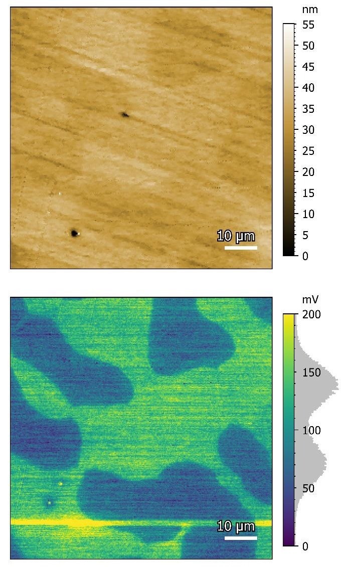
Figure 4. Stainless Steel. The top image is an 80 x 80 μm topography image while bottom image shows the KPFM signal collected simultaneously. Image Credit: Nanosurf AG
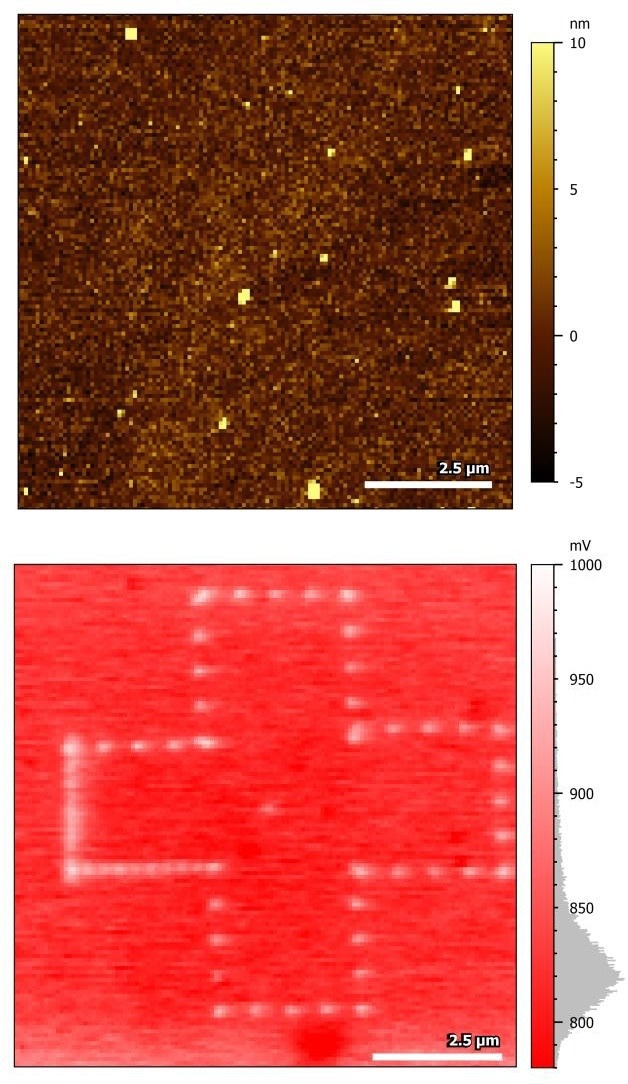
Figure 5. KPFM of locally deposited charges on an insulating oxide surface. The top image shows the surface topography while the bottom image is the KPFM image. Image Credit: Marcin Kisiel, Thilo Glatzel and students of the Nanocurriculum of the University of Basel, Switzerland.
KPFM as Improvement Tool for Other Modes
When performing dynamic mode imaging, the contact potential difference between the tip and a sample influences the cantilever oscillation. This suggests that topography measurements in heterogeneous samples in dynamic mode are impacted by contact potential variations of the sample and need to be offset.
To put it another way, the CPD heterogeneity of the materials forces an error in the measured height difference between two dissimilar materials. Using KPFM feedback throughout topographical measurements can offset any errors, improving the accuracy of AFM measurements on heterogeneous materials.
Equally, MFM measurements achieve the same result. In MFM, the phase close to the resonance frequency of the cantilever can be applied to measure the force resulting from local magnetic dipole moments. However, the phase does not differentiate magnetic forces from electrostatic forces. Applying KPFM when conducting MFM measurements will contain the effect of electrostatic forces on the phase shift, boosting the accuracy of the MFM data.

This information has been sourced, reviewed and adapted from materials provided by Nanosurf AG.
For more information on this source, please visit Nanosurf AG.