Solid oxide electrolysis cells (SOEC) show great promise as an alternative to batteries for storing excess renewable energy as they achieve almost 100% electrical-to-H2 efficiency.
In the SOEC, high-temperature electrolysis is applied to gaseous water to split it into pure oxygen and hydrogen.1 Subsequently, the resulting hydrogen may be stored and utilized as an environmentally clean, zero-emission fuel.
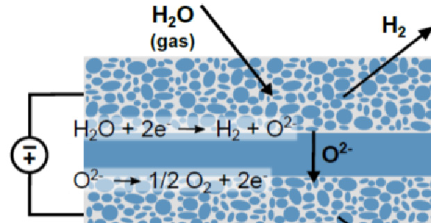
Figure 1. Schematic showing the principle of operation of a SOEC. Image Credit: Carl Zeiss Microscopy GmbH
The SOEC consists of different ceramic layers, as displayed in Figure 1. The electrolyte between the anode and the cathode is dense and a few micrometers thick, while the electrodes are thicker and porous to facilitate the transport of gases.
At the cathode side, steam is fed to the SOEC. A sufficient voltage difference is applied between the electrodes to reduce the steam at the cathode-electrolyte interface, producing oxygen ions and hydrogen gas.
These oxygen ions travel to the anode via the dense electrolyte, where they are released following oxidation as oxygen gas.
The operation of SOECs takes place at temperatures between 500 °C and 800 °C. Chemical interdiffusion at interfaces and crystallographic or morphological changes can occur at these temperatures, resulting in cell performance degradation over time.
An important goal of current research on SOECs is the extension of their lifetimes. Presently, performance loss rates are approximately a few percent per year. However, this is insufficient for the broad adoption of this novel technology, and further advancements are required.
In this context, 3D X-Ray and focused ion beam scanning electron microscopy (FIB-SEM) play a fundamental part in this advancement. They allow researchers to track changes in the device topology and morphology caused by its operation across various relevant length scales.2, 3
These changes include microstructural coarsening or the formation of undesired phases.
This article presents a study that combines FIB-SEM tomography with chemical energy dispersive spectroscopy (EDS) to examine the aging of a SOEC.
Sample
The cell imaged by FIB-SEM/EDS consists of a yttria-stabilized zirconia (YSZ) electrolyte, a heterogeneous Ni-YSZ hydrogen electrode, a single solid phase lanthanum strontium cobalt (LSC) oxygen electrode, and a gadolinia-doped ceria (GDC) compatibility layer to inhibit any reaction between the LSC electrode and the YSZ electrolyte.
The sample was extracted from a 6-cell stack operated during 11,300 hours in steam electrolysis at 710 °C and between 0.5 to 0.6 A cm-2.4
There was severe degradation during the first 2,000 hours, with an average voltage increase rate of 4%/kh, then stabilized at less than 0.5%/kh.
The stack withstood accidental water interruption incidents and was stopped after the fourth one. A cell sample was extracted from the stack and subsequently fractured to expose the interfaces between the electrolyte and the electrodes.
The sample was then impregnated with EPON812, polished mechanically, and later via ion milling.
FIB-SEM Tomography with Atlas 5
The FIB generates cross-sections perpendicular to the sample surface during FIB-SEM tomography, as shown in Figure 2a.
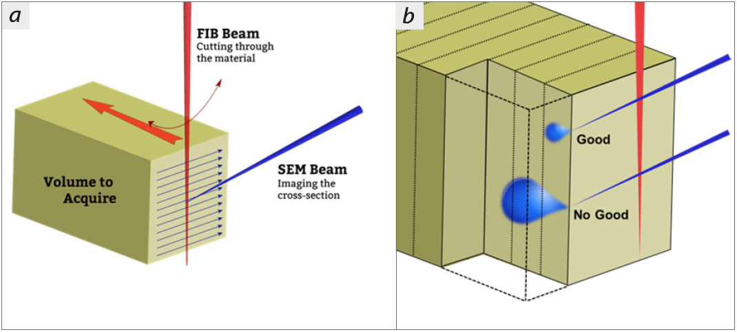
Figure 2. (a) Schematic of a sample during FIB-SEM tomography. (b) Illustration showing the VOI and volume probed by the SEM. The dotted lines correspond to the location of the different sections of the tomogram. Image Credit: Carl Zeiss Microscopy GmbH
The sample is positioned at the point of intersection between FIB and SEM beams at an angle of 54°, relative to each other. This allows the cross sections to be imaged by SEM either during or immediately after cutting without moving the sample.5
Removing a thin slice of material via FIB and imaging the newly exposed cross-section via SEM is typically repeated many times. This provides a stack of image results, each relating to one slice of the volume of interest (VOI).
A digital reconstruction of a 3D model of the VOI can be made using the image data. The 3D resolution of the FIB-SEM tomogram is set by the resolution of the SEM images (XY plane) and in the Z direction by the SEM excitation depth and the slice thickness control.
It is an excellent experimental challenge to achieve a resolution in Z that equals the XY SEM resolution of usually just a few nanometers.
To avoid signal convolution across slices, the information depth must be of the order of the targeted slice thickness, preferably smaller, as shown in Figure 2b. Energy selective backscattered (EsB) electron imaging at a low voltage (less than 2 kV) is the most surface-sensitive imaging method in SEM.
The Inlens EsB detector provides a high-pass energy filter, allowing only electrons to pass within a small energy window below the primary landing energy (low-loss electrons). These originate from regions very close to the surface.
Monte Carlo simulations demonstrate that EsB signals probe less than 3 nm deep into silicon for 1 keV landing energy and an energy window of 100 eV.6
However, 3D EDS spatial resolution is significantly lower. For a given SEM landing energy, the interaction volume for X-Ray generation is inherently greater than that for backscattered or secondary electron generation.
Although FIB-SEM tomography delivers maximal spatial resolution when conducted at low accelerating voltages, EDS demands greater landing energies for the excitation of the characteristic EDS fingerprint.
As a result, it is usually sufficient to obtain EDS data only every 5 to 20 tomogram slices, dependent on the sample, slice thickness, and elements of interest.
The advanced FIB-SEM tomography solution Atlas 5 employed for this experiment can automatically switch between two distinct sets of SEM conditions.
The first set is at low current and voltage to obtain high-resolution electron images with minimum voxel sizes. The second set is at a much higher voltage, and the current is to obtain high-throughput EDS mapping with lower spatial resolution.7
This results in 3D electron imaging resolution not being sacrificed by the EDS analysis.
This raises the question of whether it is possible to control the removal of material by FIB from the VOI to reproducibly cut slices only a few nanometers thick.
In this case, Atlas 5 utilizes fiducial marks patterned by FIB on the sample surface above the VOI, as displayed in Figure 3. Atlas 5 utilizes the central three lines to conduct drift correction, auto-stigmation, and auto-focus functions during the experiment.
The two outmost lines measure the slice thickness by the straightforward tracking of their distance change between consecutive cross sections.
Atlas 5 modifies the speed of material removal corresponding to the measured slice thickness during the run to provide homogeneously spaced sections. Isometric voxels as small as 3 nm have been reported using Atlas.8
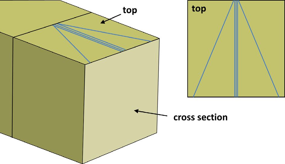
Figure 3. Perspective and top view of the VOI. The outer blue lines are fiducials used for adaptive tracking of the slice thickness. The central lines are used for drift correction, auto-focus and auto-stigmation. Image Credit: Carl Zeiss Microscopy GmbH
Experiment
The FIB-SEM tomography data from the secondary electron / secondary ion detector (SESI) and the Inlens EsB detector was recorded at an acceleration voltage of 1.8 kV on the SOEC sample.
Before this acquisition, fiducial marks were milled to modify the position of the FIB beam and ensure isometric voxels of 10 nm, with a precision in the range of 1 nm. The acceleration voltage was also automatically switched from 1.8 kV to 10 kV every 10 slices to obtain EDS elemental maps.
The EDS voxel size was selected as 40 × 40 × 100 nm³ to match in a first-order approximation the greater interaction volume when in EDS conditions. The voltage of 10 kV enables the detection of all relevant elements within the sample, such as Y, Ni, Zr, La, O, Gd, Sr, and Ce. The reconstructed volume was 38 × 10 × 11 µm3.
Figure 4 presents an example of a SESI image and the corresponding EDS dataset. A total of 1,100 sections were prepared and 110 EDS maps were collected. Each section of the tomogram was imaged, obtaining SESI and EsB signals concurrently.
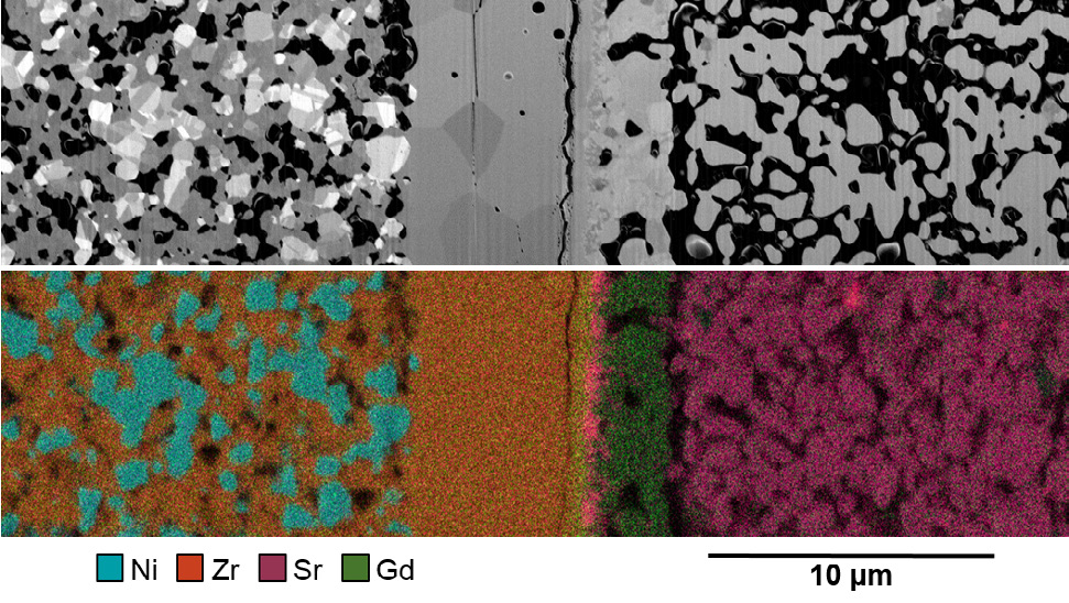
Figure 4. SESI (top) and EDS (bottom) images of an exemplary slice of the SOEC tomography dataset. Image Credit: Carl Zeiss Microscopy GmbH
The three central notches utilized for drift correction, auto-stigmation, and auto-focus during the tomography run (as shown in Figure 3) were also utilized for post-acquisition fine alignment of the electron images relative to each other.
The EDS maps were subsequently registered with the aligned SEM dataset and resampled at a voxel size of 10 nm.
Segmenting the data involves the assignment of a label to each voxel that belongs to a given material phase. This was conducted using Matlab routines with calls to Avizo software for data visualization and analysis for image gradient and watershed transform computations.
The markers for each pore, Ni, YSZ, Ce, and Sr-containing phases were created by combining the SESI and EDS datasets. Figure 5 presents a 3D view of the labeled imaged (color-coded) volume with the improvement of the markers for the watershed-based segmentation with the EDS information.
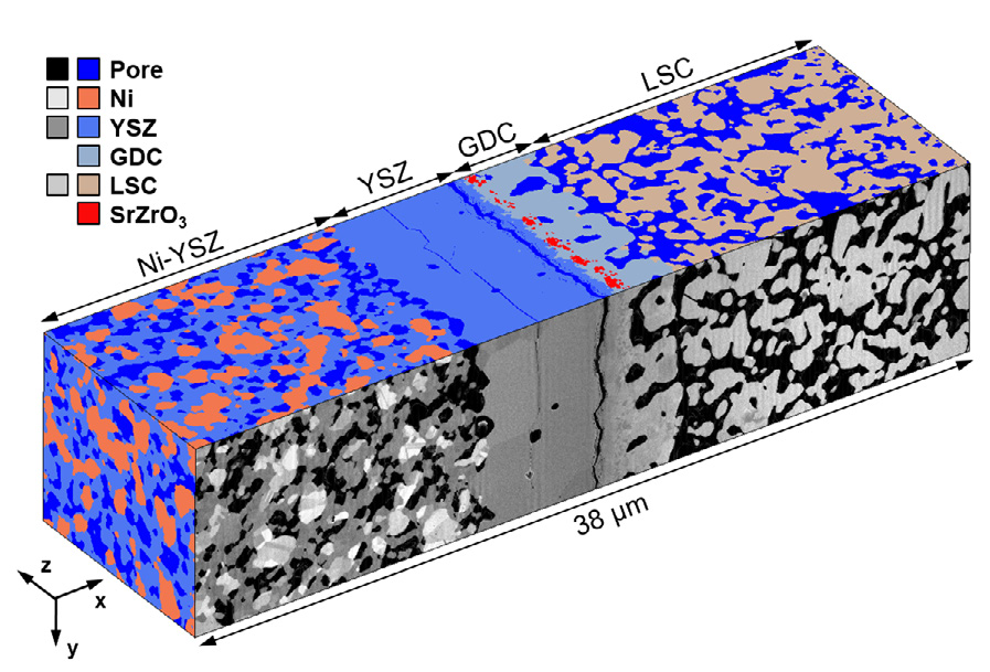
Figure 5: 3D reconstruction of the VOI. Image Credit: Carl Zeiss Microscopy GmbH
Discussion
SOEC post-test analyses exhibit improved Sr and Zr cation diffusion across the electrolyte layers, delamination, and Ni redistribution near the electrolyte. This leads to an increased degradation rate compared with solid oxide fuel cell (SOFC) conditions.
The current understanding partly rationalizes the difference in behavior qualitatively, but the precise nature of the phenomena and the driving forces continue to be imprecisely known.9,10
3D imaging at high spatial resolution with advanced capabilities for elemental mapping is fundamental to understanding the multiple transport phenomena that occur across the layers under gradients of electrochemical potential in operation.
3D elemental information improves the segmentation. Ni grains that cannot be distinguished from the YSZ phase in the SESI data due to percolation or orientation can be segmented accurately, as shown in Figure 4.
The EDS data distinguishes the GDC, YSZ, and LSC phases, as shown in Figure 5. In the 11,000-hour SOEC sample, significant microstructural degradation was observed.
The GDC interlayer partly inhibits the formation of a layer of SrZrO3 insulating secondary phase, which grows quicker than in SOFC operation and raises the ohmic losses within the cell.
This difference may result from the vacancy concentration within the oxygen electrode in SOFC and SOEC mode and/or Zr diffusion, leading to closed porosities forming along the grain boundaries in the YSZ electrolyte.
The formed secondary phases and closed porosity impact the cell’s resistance to thermal cycling. In the current sample, the weakened interface led to delamination over a sizable area that hinders the transport of oxygen ions.
Despite cracking possibly occurring during sample preparation or uncontrolled water interruption events, similar failures are not usually seen in pristine and SOFC samples.
These observations suggest that the development of cost-effective techniques for depositing dense interlayers, and likely controlling the oxygen vacancy concentration in the oxygen electrode by manipulating the SOEC stack operating conditions, are crucial for extending the lifetime of SOEC devices.
Micro-cracking is observed in the LSC electrode, while inter-phase cracks are observed in the Ni-YSZ electrode, mostly near the YSZ electrolyte.
The contiguity of the phases is not significantly impacted, but the cracks may impact the transport pathways to the electrocatalytic sites locally within the electrochemically active regions.
The transport properties of the Ni phase and the density of triple-phase boundary sites in the Ni-YSZ are impacted by microstructural coarsening. The depletion of Ni is observed near the YSZ interface in the current sample. Currently, the precise reasons for micro-cracking and Ni depletion are still unknown.
Conclusion
Advanced FIB-SEM tomography was employed to reveal structural changes in an aged SOEC. The chemical EDS information provided in the 3D dataset enabled the correct segmentation of the different phases present in the sample. This was vital to better understand the mechanisms causing cell deterioration.
The 3D FIB-SEM/EDS's capability allows the measurement of topological and metric properties. It directs discrete-element simulations to accurately quantify microstructural changes' extent and their detrimental effect on cell performance.
These analyses will soon be conducted on the segmented data to provide an enhanced understanding of SOEC degradation and provide precise guidance for microstructural design and stack operation strategies.
Acknowledgments
Produced from materials originally authored by Marco Cantoni from the Centre Interdisciplinaire de Microscopie Électronique, École Polytechnique Fédérale de Lausanne (EPFL); Arata Nakajo, Giorgio Rinaldi, Stefan Diethelm, and Jan van Herle from the Institute of Mechanical Engineering, SCI-STI-JVh Group of Energy Materials (GEM), École Polytechnique Fédérale de Lausanne (EPFL); and Fabián Pérez-Willard from Carl Zeiss Microscopy GmbH.
References and Further Reading
- A. Vojvodic and J. K. Nørskov, Optimizing Perovskites for the Water-Splitting Reaction, Science 334 (2011), pp. 1355-1356.
- J.R. Wilson et al., Three-Dimensional Reconstruction of a Solid Oxide Fuel Cell Anode, Nat. Mater. 5 (2006), pp. 541–544.
- G.J. Nelson et al., Comparison of SOFC cathode microstructure quantified using X-ray nanotomography and focused ion beam-scanning electron microscopy, Electrochem. Commun., 13 (2011), pp. 586-589.
- G. Rinaldi et al., Post-test Analysis on a Solid Oxide Cell Stack Operated for 10,700 Hours in Steam Electrolysis Mode, Fuel Cells (2017) in press.
- M. Cantoni and L. Holzer, Advances in 3D focused ion beam tomography, MRS Bulletin 39 (2014), pp. 354-360.
- Not shown. Results were obtained using the Monte Carlo simulation software CASINO. See: D. Drouin et al., Scanning 29 (2007), pp. 92-101.
- K. Narayan et al., Multi-resolution correlative focused ion beam scanning electron microscopy: applications to cell biology, J. Struct. Biol. 185 (2014), pp. 278-284.
- M. Cantoni et al., Proceedings of the 16th European Microscopy Congress, Lyon, France (2016).
- F. Tietz et al., Degradation phenomena in a solid oxide electrolysis cell after 9000 h of operation, J. Power Sources 223 (2013), pp. 129-135.
- D. The et al., Microstructural comparison of solid oxide electrolyser cells operated for 6100 h and 9000 h, J. Power Sources 275 (2015), pp. 901-911.

This information has been sourced, reviewed and adapted from materials provided by Carl Zeiss Microscopy GmbH.
For more information on this source, please visit Carl Zeiss Microscopy GmbH.