Graphene is a material that has a one-atom layer of carbon atoms with a thickness of only 335 pm. It can be modified using oxidization and functionalization. For example, graphene gains properties such as water solubility, which is beneficial for further device processing.
Functional groups can also change the interaction with other materials, which is needed for the integration and interfacing of transistors, solar cells, and batteries.
The controlled modification of graphene remains a challenge and requires assessment using a scanning electron microscope and Raman spectroscopy. In situ Raman and scanning electron microscope (SEM) studies provide valid complementary information.1
Raman spectroscopy is the preferred analytical technique for examining functional groups, edge and grain boundaries, defects, strain and thermal conductivity, doping, and the quality of the reduction process.
SEMs produced by ZEISS provide high-resolution images, proper contrasting methods, and a high depth of field.
These SEMs allow the fast and simple differentiation between one-layer, two-layer, and multi-layer graphene, in addition to the different graphene types, particularly when employing the Inlens EsB detector.2
Measurements
Raman spectroscopy and SEM were applied to provide information regarding mechanically exfoliated graphene, liquid exfoliated graphene oxide, and reduced graphene oxide.
The Inlens SE-detector was utilized in the ZEISS FE-SEM. Here, the secondary electrons deliver an adequate signal to image the different types of graphene.
This imaging was alternated with Raman analysis, carried out by a Renishaw inVia Raman microscope equipped with a 532 nm laser in conjunction with the FE-SEM, via a Renishaw SEM-SCA interface.
An interesting area was repeatedly defined on the SEM image and a Raman spectrum was created from the same spot.
During this experiment, the SEM-SCA interface was placed below the SEM’s pole piece, resulting in an SEM working distance of 14 mm. As a result, the SEM image remains visible following the insertion of the SCA interface, delivering a consistent analysis point in the SEM.
Challenge
The key peaks in the graphene Raman spectrum are D, 2D, and G. The number of layers can be determined from the ratio of peak intensities, 2D/G, and the shape and position of these peaks.
Using the ratio of peak intensities D/G, Raman spectra can be utilized to characterize the level of disorder in graphene.3–6 Due to the hexagonal structure of the graphene lattice, ordered crystal edges have two main structures: armchair and zigzag.7, 8
Only armchair edges can elastically scatter charge carriers to produce the D peak.7, 8 However, defects lead to these peaks expanding, which may decrease the intensity and additional peaks arising in the spectrum. This makes it challenging to interpret peak positions and ratios.9
However, the Raman ID/IG ratio may be employed to estimate the mean defect distance of densely packed point defects in graphene, utilized in the evaluation described here.10
The carbon atoms may be sp3-hybridized, functionalized, oxidized, or missing. Integrating the Raman system into the ZEISS FE-SEM allowed Raman and SEM measurements to be co-located, which is vital for this work. Before the analysis, the electron and laser beams must be accurately aligned.1
Results

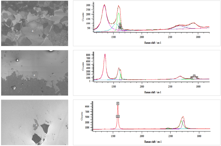
Figure 1. SEM images and the respective Raman point measurements at point a. Image Credit: Carl Zeiss Microscopy GmbH
Graphene oxide on SiO (as shown in Figure 1, top) displays large flakes up to 30 μm across the SEM. The GO material is comprised of randomly aggregated, overlapping, closely associated thin sheets.
The layers at the measured spot have a defect density of around 50%, meaning that every second carbon atom has sp3-hybridization.10
A higher defect density results in a more sensitive material to acceleration voltages. The 3 kV utilized in this study led to the graphene being damaged and likely contributed to the high defect rate. A voltage of at least 0.5 kV is recommended to be used in the future.
The reduced graphene oxide (as shown in Figure 1, middle) is seen to be an almost closed layer. The Raman spectrum indicates that the rGO has fewer defects, with a defect density of approximately 1%, meaning that every 100th atom has a defect.11
Graphene that has fewer defects is expected to be more resistant to electron damage but, as demonstrated by the SEM image, an interaction with the material has likely changed its properties.
The mechanically exfoliated graphene on silicon oxide (as shown in Figure 1, bottom) is essentially graphite and not graphene. It does not appear as a continuous layer or overlapping layers but instead as single flakes. There is a minimum of 10 layers and the defect rate is approximately 0%.
The SEM image in general displays lower resolution and contrast due to the required working distance to accommodate the SCA (14 mm) but is easily satisfactory for scientific investigations.
Raman bands are not as intense as in a modular Raman spectroscope because of the parabolic mirror and optical fibers. However, the interpretation of the spectra by peak position and shape is straightforward.
Conclusion
The detection of the different graphene states was easily carried out using this in situ SEM Raman method. The advantage of the integrated system is the high-resolution SEM imaging (including alternative detectors) alongside the chemical analysis delivered by Raman spectroscopy.
The highly accurate co-location of the electron beam and laser spot provides reliable results that are easy to interpret.
Acknowledgments
Produced from materials originally authored by Isabel Guerra at Tschuschke University Granada, Centro de Instrumentación Científica, Spain; Sébastien Maussang and David Reece at Renishaw Ibérica, S.A.U, Spain; Philipp Vecera, Siegfried Eigler, Andreas Hirsch, and Frank Hauke at FAU Erlangen-Nürnberg, Zentralinstitut für Neue Materialien und Prozesstechnik (ZMP), Germany; and Stefanie Freitag at Carl Zeiss Microscopy GmbH, Germany
References and Further Reading
- I. Guerra, Journal of Microscopy, 2015
- V. Mikhailovskii and O. Vyvenko, Interdisciplinary Resource Center for Nanotechnology St. Petersburg State University, Russia
- Ferrari, A. et al, A. K. Phys. ReV. Lett. 2006, 97, 187401.
- Graf, D. et al, Nano Lett. 2007, 7, 238.
- Yan, J. et al, Phys. ReV. Lett. 2007, 98, 166802.
- Pisana, S. et al, Nat. Mater. 2007, 6, 198
- You, Y. et al, Appl. Phys. Lett. 2008, 93, 163112
- L.M.Malard et al, Physics Reports 473 (2009) 51 – 87
- L.G. Cancado et al, Nano Lett., 2011, 11 (8), pp 3190 – 3196
- Jan M.Englert et al, ACS Nano, 2013, 7 (6), pp 5472 – 5482
- Eigler S. et al, Adv. Mater. 2013, 25 (26), 3583 – 3587

This information has been sourced, reviewed and adapted from materials provided by Carl Zeiss Microscopy GmbH.
For more information on this source, please visit Carl Zeiss Microscopy GmbH.