Sponsored by Nanosurf AGReviewed by Olivia FrostJan 24 2024
The world of nanoscale analysis has been revolutionized by the advent of electrical Atomic Force Microscopy (AFM) modes. New possibilities for measuring electrical properties with remarkable precision have been unlocked by these techniques.
These modes, from Conductive AFM (C-AFM) to Kelvin Probe Force Microscopy (KPFM) and Piezoresponse Force Microscopy (PFM), have found wide applications across a range of industries, including semiconductor technology, materials science, energy storage, and life sciences.
In this article, a comprehensive overview of the history, principles, and applications of electrical AFM modes is provided, underscoring their crucial role in enhancing the global understanding of materials and devices at the nanoscale.
Tracing the Evolution: History and Background
The late 1980s and early 1990s saw the true journey of electrical AFM modes begin following the invention of the AFM in 1986. Today, these modes have evolved to measure a wide array of electrical properties, including surface potential, conductivity, and piezoelectric response.
The basic principle of AFM is mirrored in the operational principle of electrical AFM modes: a sharp probe approaches a sample surface, and a measurement is taken of the interactions between the probe and the sample.
However, an additional bias voltage is applied either to the probe or the sample in electrical AFM modes, and the resulting electrical response is measured. This response can manifest as a force, a current, or a displacement, depending on the specific mode.
Broad Spectrum of Applications Across Industries
Electrical AFM modes such as CAFM/SSRM, KPFM, PFM, EFM, and SMM, along with MFM, are widely used across various industries. They play a crucial role in enhancing our knowledge of nanoscale electrical properties.
Semiconductor Industry
Electrical AFM modes, particularly C-AFM/SSRM, KPFM, and SMM, are indispensable in the semiconductor industry.
C-AFM/SSRM is used to investigate the conductivity of nanoscale transistors, leading to the development of ultra-low power transistors for device characterization and material analysis. KPFM, meanwhile, provides insights into the distribution of energy levels across the surface of semiconductor materials, where it assists in refining the fabrication processes.
On the other hand, SMM offers unique capabilities for the non-destructive characterization of subsurface structures, which is essential for quality control and failure analysis (Fig. 1). This has assisted in the improvement of the overall yield of semiconductor production lines.
Materials Science
EFM, MFM, PFM, and SMM are extensively employed in materials science for exploring novel materials. PFM has been crucial in the study of the piezoelectric properties of polymers, which has led to the development of high-performance piezoelectric sensors and actuators.
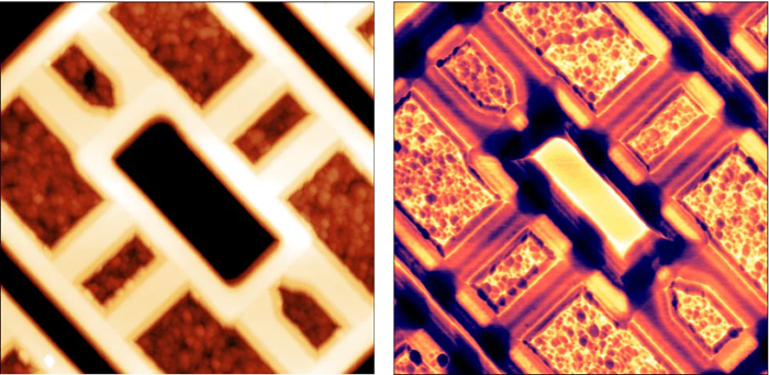
Figure 1. Topography (left), Im (S11) or capacitance (right) of an SRAM sample. Scan size is 10 x 10 μm2. Image Credit: Nanosurf AG
EFM is a benefit when it comes to understanding the charge-trapping phenomenon in organic semiconductors, which improves the stability of these materials. With its ability to probe local dielectric properties, SMM has been instrumental in characterizing complex material systems, like multiferroics and ferroelectric thin films.
This has, in turn, led to the development of novel multifunctional devices. MFM assists with understanding magnetic domain arrangements and changes and is vital and irreplaceable for investigating nanoscale magnetic structures in novel materials.
Energy Industry
C-AFM and SMM are emerging as influential tools in the energy industry. C-AFM, in particular, is being used to study conductivity and ion transport in solid electrolytes of advanced lithium-ion batteries. This has been crucial in creating safer, more efficient lithium-ion batteries.
SMM’s capability to examine dielectric properties plays a pivotal role in understanding materials’ behavior under actual operating conditions. This insight is essential for developing more durable and efficient fuel cells.
Life Sciences
Electrical AFM modes like C-AFM and SMM have also made significant contributions to life sciences. C-AFM has been instrumental in examining neuronal electrical conductivity, deepening our understanding of cellular-level neural communication and aiding advanced neuroprosthetics development.
Meanwhile, SMM’s ability to assess local permittivity has offered fresh perspectives on cellular processes, furthering our knowledge of biomaterials and biological systems and supporting the creation of innovative drugs and treatments.
Data Storage
In the development of advanced data storage technologies, electrical AFM modes such as MFM, CAFM, and SMM have proven invaluable. MFM has been used to study the nanoscale magnetic domains in hard disk drives (Fig. 2), leading to notable enlargements in storage density.
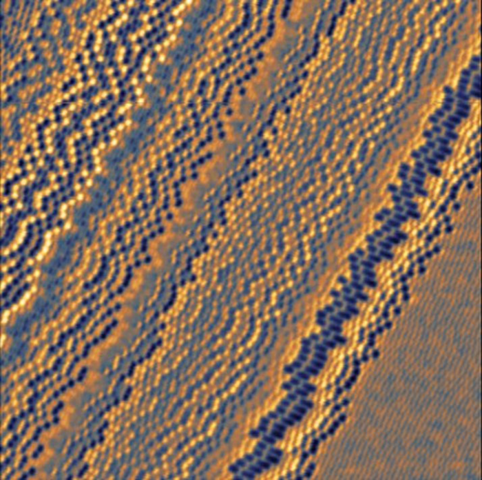
Figure 2. MFM image showing the data stored in a hard disk drive. Hard disc drives remain to be the choice of preference for long-term data storage in servers. MFM is used both during the development of new drives and as part of the quality control process. Image size: 11 x 11 μm2. Image Credit: Nanosurf AG
While SMM, with its ability to probe subsurface features, offers unique advantages in the characterization of memory devices, C-AFM has been employed in the investigation of the electrical properties of magnetic recording media.
This has contributed to the creation of next-generation high-density storage systems, including advanced solid-state drives with increased reliability and data retention properties.
Understanding the Modes
Conductive Atomic Force Microscopy / Scanning Spreading Resistance Microscopy Conductive Atomic Force Microscopy (CAFM) was first developed at the University of Cambridge in 1993.
This mode evaluates the localized electrical properties of a material. In this mode, the probe is coated with a conductive material, and it is this probe that acts as a nanoscale electrode. The sample is facilitated when a bias voltage is applied to the flow of a current from the tip.
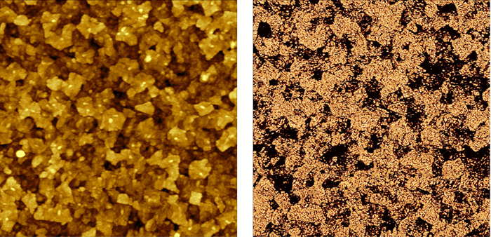
Figure 3. Topography (left) and a C-AFM image (right) of an ITO thin film on glass substrate. Image size: 5 x 5 μm2, current range: 12 nA. Image Credit: Nanosurf AG
Measurements are taken of the current flowing between the probe and the sample, which offers insights into the local electrical conductivity or – in other words – evaluates the resistance of the local tip-sample contact (Fig. 3).
In C-AFM measurements, a DC voltage is applied to the tip, and the resulting current is measured. This current is transformed into a voltage signal using a linear transimpedance amplifier, capable of handling a current range spanning 4-5 decades.
However, certain applications, like in semiconductor heterostructures, demand broader current ranges (up to 7-8 decades). This is achievable with a logarithmic transimpedance amplifier. C-AFM equipped with such an amplifier is known as Scanning Spreading Resistance Microscopy (SSRM).
The name Scanning Spreading Resistance Microscopy originates from the early days of the semiconductor industry, and the word microscopy was added to the existing measurement of scanning spreading resistance when the mode became available in modern AFMs.
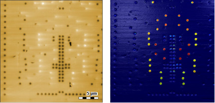
Figure 4. Topography (left) and a C-AFM image (right) of an interconnect structure. The C-AFM image shows different conductivities for different groups of contacts. Image size: 25 x 25 μm2, current range: 1.5 nA. Image Credit: Nanosurf AG
C-AFM and SSRM are crucial for analyzing solid materials, nano- and microscale electronic devices, conductive polymers, nanoparticles, thin films, biological samples, and nanostructures down to single molecules.
They are extensively used in the solar cell and semiconductor industries for a variety of high-resolution measurements, such as material characterization, semiconductor dopant profiling, and quality control of dielectric films and oxide layers.
An additional aspect of C-AFM involves measuring the local current-voltage characteristics at the tip-sample contact. This technique reveals information about the sample’s conductivity type, whether it’s dielectric, semiconductor, semimetal, or metal.
Electrostatic Force Microscopy (EFM)
Electrostatic Force Microscopy (EFM) measures the electrostatic force acting between the probe and the sample, thereby revealing information about local surface potential and charge distribution.
To achieve this, an electrically coated probe is oscillated at its resonance frequency, maintaining a non-contact state with the sample. In this mode, the oscillating cantilever becomes sensitive to long-range electrostatic force gradients.
Change in the cantilever’s resonance frequency is caused by changes in the potential difference between the tip and sample. This, in turn, causes a change in the phase response at the excitation frequency.
EFM is particularly useful in understanding charge trapping and charge transport phenomena in semiconductors and dielectric materials.
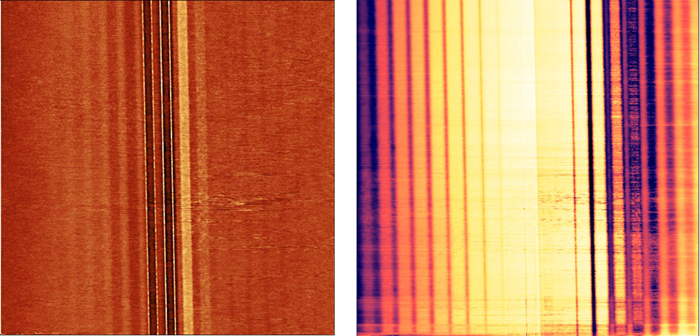
Figure 5. Topography (left) and an SSRM image (right) of a dopant density calibration sample. SSRM image shows different conductivities for regions with different dopant densities. Range of dopant densities: 4x10¹⁵ – 1020 cm-3. Image size: 50 x 50 μm2, current range: 15 μA. Image Credit: Nanosurf AG
Kelvin Probe Force Microscopy (KPFM)
Kelvin Probe Force Microscopy (KPFM) is a technique that assesses the contact potential difference (CPD) between the conductive AFM probe and the sample. This difference, rooted in their varying work functions, offers crucial information about the sample’s surface potential, thereby providing valuable insights into its electronic structure.
Typically, KPFM operates by imaging the sample in dynamic mode and further exciting the cantilever probe electrically at an additional, different frequency to determine the CPD.
A further feedback loop analyzing the mechanical cantilever response to the electrical AC excitation controls the DC tip bias and, in so doing, determines the CPD between tip and sample by reducing the electrostatic forces acting between tip and sample.
KPFM enables the mapping of local CPD and, consequently, the work function across a sample’s surface. This capability is essential for investigating aspects like material distribution, which are not discernible through topographic imaging, as well as studying corrosion, semiconductor materials, thin films, and 2D materials. For instance, Fig. 6 (left) displays semi-fluorinated alkanes that are barely visible in topographic images but are clearly identifiable using KPFM.
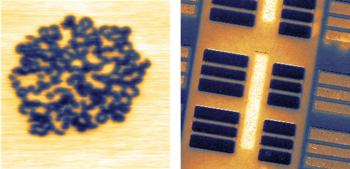
Figure 6. KPFM images of the self-assembly of semi-fluorinated alkane molecules F(CF2)14(CH2)20H (F14H20) on mica (left) and an SRAM sample showing regions with different carrier doping (right). Both images were recorded by single pass AM KPFM on 2nd eigenmode. Image sizes: 2 x 2 μm2 (left) and 40 x 40 um2 (right). Image Credit: Nanosurf AG
In semiconductor materials, regions with different dopant levels appear to have different surface potentials (Fig. 6, right). This way, KPFM can be used to identify materials, evaluate the effect of treatments on the conductivity, localize defects (e.g., impurities embedded within the substrate), or recognize parts of a circuit that are not electrically connected.
KPFM is also instrumental in exploring novel 2D materials. Its applications include characterizing chemical doping in graphene for chemical sensors, determining layer count, assessing electrical properties of stacked 2D materials and their interactions with substrates, and evaluating the purity of grown materials.
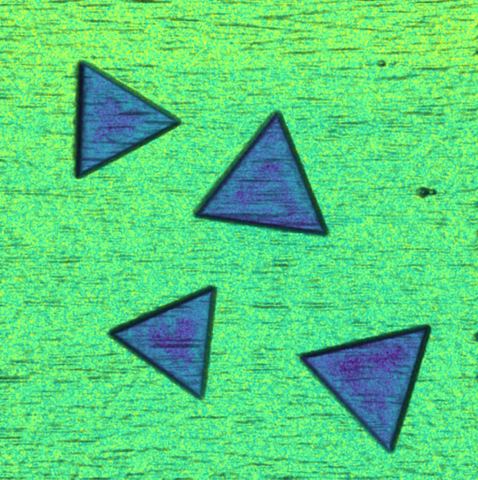
Figure 7. KPFM image showing 2D crystals of MoS2 on silicon oxide. The image was done by off-resonance single pass AM KPFM. Image size: 42 x 42 μm2. Image Credit: Nanosurf AG
The MoS2 flakes shown in Fig. 7 appear to be very similar at first glance, but KPFM imaging reveals subtle differences in the CPD in the center of the flakes that might point toward lattice defects or impurities.
Piezoresponse Force Microscopy (PFM)
PFM, or Piezoresponse Force Microscopy, is a powerful technique used to investigate the piezoelectric response of materials. A fascinating property is exhibited by piezoelectric materials: they generate a voltage when subjected to mechanical deformation, and they deform, conversely, when exposed to an electrical field.
This quality makes piezoelectric materials useful in a wide variety of applications ranging from biomedical (e.g., ultrasound, auditory, or biosensors) to advanced electronics (e.g., energy production, data storage, or sonar equipment).
The phenomenon of the reverse piezoelectric effect is leveraged by PFM to study piezoelectric materials at the nanoscale.
Applying an alternating voltage (VAC) between the sample and the conductive tip of an AFM probe instigates a deformation of the sample in PFM. Measurements are taken of the resulting change in the probe’s deflection at the frequency of the alternating voltage, which provides valuable information about the amplitude and phase of the piezoelectric response.
Amplitude and phase report the amount of a material’s extension and its orientation (polarization) inside the sample, respectively. The study of ferroelectric materials, piezoelectric thin films, and advanced sensor and actuator materials have all provided extensive applications for this feature of PFM.
The practical applications of PFM can be observed in the study of various materials, for instance. PFM has been used to extensively investigate one particularly common piezoelectric material, lead zirconate titanate (PZT), and an optically transparent material commonly used in piezo sensors and mobile phones, lithium niobite (LiNbO3).
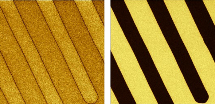
Figure 8. CR-PFM on LiNbO3: PFM amplitude (left) and PFM phase (right). In the PFM amplitude image, the piezoelectric domain boundaries are clearly visible while the PFM phase image indicates the polarization direction of the domains. Image size: 30 x 30 μm2. Image Credit: Nanosurf AG
Figure 8 displays an example of periodically poled LiNbO3 imaged in PFM exploiting the contact resonance of the cantilever to amplify the piezoelectric response of the material.
VAC is applied at the cantilever’s contact resonance, which allows smaller VAC to be applied or thin or weakly responsive materials to be investigated.
At domain boundaries, the deformation in response to the VAC is minimal, allowing the amplitude image to distinctly reveal these structures. The phase image indicates the orientation of piezoelectric domains. A change in domain orientation results in a 180° phase signal shift, as the sample’s deformation aligns either in-phase or counter-phase with VAC.3
In ferroelectrics, Switching Spectroscopy (SS) PFM is used to probe the switching voltage for the electrical polarization. VAC is applied to measure the piezoresponse during the measurements, usually at or close to the contact resonance frequency.
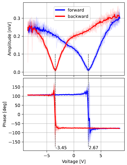
Figure 9. Highly reproducible (11 repetitions) SS-PFM measurement on a BaTiO3 thin film sample at the contact resonance frequency. The amplitude and phase for all measurements were plotted for the voltage “off” state, showing the remanent polarization, with the thick curve representing the average of those curves. Image Credit: Nanosurf AG
The static bias voltage (VDC) is cycled between “off” (VDC=0) and “on” states, where the “on” state voltage is ramped up at each switching event to measure remanent polarization. Though the voltage applied during the “on” state affects the local polarization, the polarization measured in the “off” state shows the remanent state polarization, which could be different from that when the voltage is applied.
This procedure allows for the determination of the voltage at which the remanent state polarization is reversed: the switching voltage.
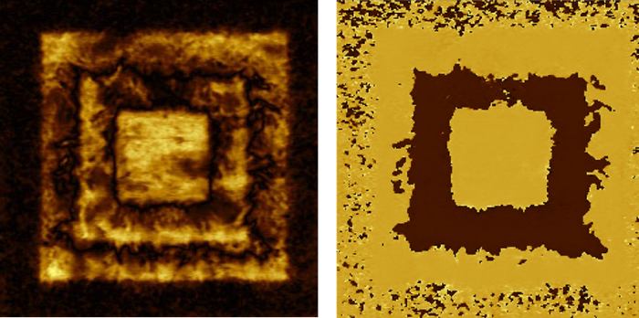
Figure 10. PFM amplitude (left) and phase (right) of P(VDF-TrFE) thin film after applying DC sample bias of 40 V, 40 V, and 40 V during consecutive scanning of 3x3 μm2, 2x2 μm2, and 1x1 μm2 areas respectively. Amplitude range: 10 pm; Phase range from -90° to 90°. Sample courtesy: Joanneum Research Forschungsgesellschaft mbH, Austria.
Typical amplitude and phase responses of an SS PFM experiment are displayed in Figure 9. The switching voltages depend on the direction of the VDC bias change and are categorized by the minima in the amplitude curves and the 180° phase changes in the phase curves.
Bias voltages exceeding the voltage levels available in the AFM scan head may be required to reach the coercive field for switching. In cases such as these, a high-voltage amplifier is connected to a user output of the AFM controller, and bias voltages (VDC) up to ±200 V can be applied (Fig. 10).
Furthermore, in order to improve the signal-to-noise ratio of weak piezoelectric properties, the excitation voltage (VAC) can also be applied via the high-voltage amplifier. The sample must be stable under high voltage to perform HVPFM and to prevent physical harm to the user or damage to electronic equipment. Care must be taken to ensure that no electronics are exposed to the high voltages applied to the sample.
Through the myriad possibilities offered by PFM, valuable insights are gained by researchers into the piezoelectric properties of materials. This knowledge enables a deeper understanding of their behavior and supports advancements in various fields, including device fabrication, materials science, and nanotechnology.
Scanning Microwave Microscopy (SMM)
A microwave signal is transmitted through a solid metal tip to the sample in Scanning Microwave Microscopy (SMM).
A fraction of the microwave signal is reflected at the surface and subsequently collected through the same tip. The so-called S11 parameter, or the ratio between the incident and reflected signal intensity, is a measure of the complex microwave impedance at the tip-sample interface. The impedance contains information about the local dielectric constant, capacitance, conductivity, and dopant density (Fig. 11).
Thus, SMM supersedes scanning capacitance microscopy (SCM), as it is more modern, and the technology is more sensitive than SCM. Similarly, like C-AFM, SMM can be applied to a wide range of materials ranging from dielectrics to metals and applications areas from semiconductors to materials research and even biological research.
The most significant application of SMM, alongside C-AFM and SSRM, lies in quality control and failure analysis of semiconductor structures (as shown in Figs. 1 & 12). Unlike C-AFM or SSRM, SMM can provide clear contrast even when the structures are obscured by an insulating oxide layer, showcasing SMM’s subsurface imaging capabilities.
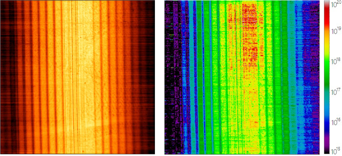
Figure 11. S11 amplitude (left) and dopant density map (right) of an Infineon SCM calibration sample with dopant densities in a range of 4x10¹⁵ – 1020 cm-3. Scan size is 50 x 50 μm2. Image Credit: Nanosurf AG
As a side effect, sample preparation for SMM and imaging reproducibility are simpler than for C-AFM or SSRM.
Regarding calibrated measurements for e.g. dopant density calculations, SMM is also more robust than C-AFM or SSRM for the same reasons. Successful processing of SMM images does, however, require basic knowledge of microwaves and the physics of the measurement.
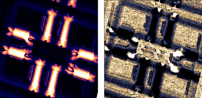
Figure 12. dS/dV amplitude (left) and phase (right) or an SRAM sample. The bright regions in the amplitude image are the p-type conducting channels. Image size: 11 x 11 μm2. Image Credit: Nanosurf AG
SMM has two different operating modes. One is the S11 measurement, which is described above. The other one is the dS/dV measurement, where an external AC voltage modulates the S11 parameter.
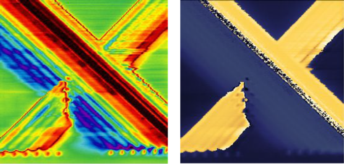
Figure 13. dS/dV amplitude (left) and phase (right) of an SCM calibration sample. The amplitude non-linearly depends on dopant density, with a maximum around 1017-1018 cm-3, and the phase change indicates the change of the type of dopants – n or p. Image size: 40 x 40 μm2. Image Credit: Nanosurf AG
Such a mode is useful while studying non-linear materials, like piezo-electrics or semiconductors. For example, in semiconductor heterostructures, a phase flip in dS/dV signal indicates a change of the dopant type i.e., n or p (Figs. 12 & 13).
Magnetic Force Microscopy
Magnetic Force Microscopy (MFM) utilizes magnetically coated AFM probes and a dual-pass imaging mode to detect stray magnetic fields above the sample surface.
In the first pass of dynamic mode, MFM measures the sample’s surface topography. Here, the van der Waals force is predominant, with magnetic and electrostatic forces present but weaker. In the second pass, at a set lift height, the probe retraces the initially recorded topography. At this height, electric and magnetic forces, decaying at a slower rate (1/r² and 1/r³, respectively) compared to the van der Waals force, become more significant.
It is then possible, by measuring the phase shift between the AC excitation signal and the recorded AC cantilever deflection, to obtain an image that is proportional to the gradient of the stray magnetic field (in other words, to visualize the edges of the magnetic domains).
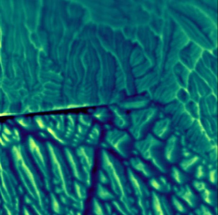
Figure 14. Left: MFM image, showing phase contrast generated by the stray fields of magnetic domains in electrical steel. By varying in-plane magnetic fields, it is possible to study the evolution of magnetization and thus understand the origin of losses in electrical transformers or motors. Image size: 100 x 100 μm2. Image Credit: Nanosurf AG
Some of the many applications of MFM include studies of thin films of magnetic coatings in magnetic hard discs (Fig. 2 right), studies of the magnetic behavior of electrical steel, which is used in, e.g., transformers for electricity transmission (Fig. 14), or studies of magnetization within micro or nanoscale magnets (Fig. 15).
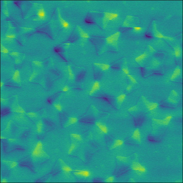
Figure 15. MFM image of stray magnetic fields between the nanomagnets in artificial spin ice. Arrays of nanomagnets are being used in neuromorphic devices to mimic how the brain operates in order to increase computation capabilities without scaling up power consumption. MFM, and variable magnetic field sample holders were used to study the evolution of these magnetic structures and how they interact with each other. Image size: 13 x 13 μm2. Image Credit: Nanosurf AG
Conclusion
To conclude, electrical AFM modes, with the recent addition of SMM, have emerged in recent years as powerful tools for nanoscale analysis. These modes can offer detailed insights into the electrical properties of materials.
Their importance in the development and manufacturing of a multitude of products and technologies is underscored by their diverse applications across various industries. These modes promise to unlock new possibilities in nanoscale analysis as they continue to evolve, paving the way for future advancements in numerous fields.
Continuous refinement and innovation in these techniques will permit us to look forward to a future offering an even deeper understanding of materials and devices at the nanoscale, with breakthroughs that could revolutionize human lives d visible on the horizon.

This information has been sourced, reviewed and adapted from materials provided by Nanosurf AG.
For more information on this source, please visit Nanosurf AG.