The world's need for data is growing at a steady rate, with new applications emerging every week. Even at the height of the COVID-19 pandemic in 2020, data consumption increased by more than 20%, highlighting the importance of efficient information routing and transmission.
The photonics industry is also rapidly expanding, with its technologies used in a wide range of mainstream applications.
These include various light detection and ranging (LiDAR) systems and sensors in wearables and vehicle cameras, as well as functions in quantum computing, high-speed cables, and even photonic computing, which uses photons instead of electrons for logic.
Silicon photonics (SiPh) is the technology that drives these advancements, combining optics and electronics on the same wafer to give considerable performance advantages in a smaller end product.
Based on the rising and diverse applications of SiPh, particularly the rise of consumer applications, production quantities will need to increase 1000-fold over the next several years to meet demand. This article examines the most recent advances in alignment automation that will help make this happen.
The Difference Between Optics and Electronics
All optical circuits must be tested, beginning with the wafer and progressing through numerous phases of construction. This necessitates significantly higher physical accuracy than probing electrical circuits, frequently by two to three orders of magnitude, as well as more degrees of freedom (DOF).
While probes can easily reach electrical test points, pad sizes of about 30 microns are practical targets for SiPh structures, which require accuracy between 20 and 50 nanometers, necessitating the development of innovative precision methods.
This precision cannot be achieved using cameras or microscopes, and alignment must be 'active', which means that placement must be based on optimizing optical power.
The Challenge of Upscaling SiPh Production
The fabrication of photonic integrated circuits requires very difficult nanopositioning tasks, and vision- or fixturing-based techniques are insufficient, especially given device variations.
The requirement for repetitive alignment throughout all manufacturing stages, from initial probing and grading on the wafer to final assembly and packaging, which includes multiple steps of placing and bonding functional elements interspersed with additional testing, has long been regarded as a barrier to scaling up production, accounting for up to 80% of total costs.
The traditionally high cost of active alignment systems has been a major motivator for the multi-decade search for passive alignment technology. However, precision active photonics alignment is now available, eliminating numerous associated expenses and allowing for a cascade of savings throughout the manufacturing workflow.
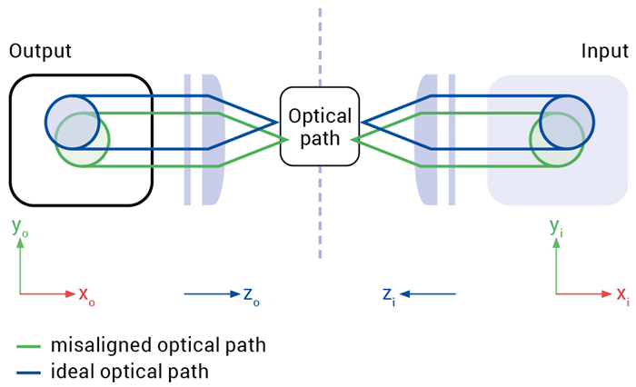
Figure 1. Testing and packaging today’s photonic devices can be a huge challenge across multiple DOFs. The alignment of multi-channel devices, such as fiber-optical arrays, used to be a slow, repetitive process before modern parallel algorithms were developed. Image Credit: PI (Physik Instrumente) LP
Passive or Active Alignment?
Precision alignment in non-photonics manufacturing can be accomplished by an active or passive technique.
A dovetail joins two boards at right angles, with the edges completely aligned. However, passive placement is frequently ineffective for applications that require higher accuracy, such as aligning optical fibers to chips or other components, because the tolerances are too tight, making manufacturing processes unstable.
As the design becomes more technical, the machine tools and procedures needed to meet the requisite tolerances become more expensive, and reject rates increase, resulting in additional expenditures.
Some device tolerances, such as fiber-core centration, cannot be addressed with improved fabrication techniques, and machining the world's finest V-groove is of little use when device-to-device variability exceeds the required alignment tolerances.
Novel passive alignment solutions have emerged that show great promise for specialized applications, such as the Photonic-Plug (Teramount), although active alignment will remain necessary.
In comparison, active alignment enhances performance by using robots to autonomously align devices, and given its cost savings, flexibility, and speed, it will likely remain the favored choice for photonic device manufacturing.
Active alignment works by maximizing coupling performance, and the latest breakthrough detailed in this article does so cost-effectively across multiple channels in different DOFs, which is necessary because SiPh can print several circuits with multiple inputs and outputs on a single chip.
Active Alignment: What is Necessary?
Active alignment requires advanced control electronics and high-precision mechanics. During the manufacturing process, the photonic device's components are autonomously controlled to maintain their mutual position.
Traditionally, this was time-consuming because optimizing several channels, inputs, and outputs across multiple DOFs required numerous iterations to achieve the desired result. Using old methodologies, the necessary time will only increase as devices become smaller and more complex, raising the cost even higher.
Alignment in a multi-lens assembly, for example, is significantly more difficult than for a single element, as is a SiPh chip with several channels rather than the single fibers used in the late 1990s.
Fortunately, revolutionary control algorithms can now simultaneously complete all of the necessary sub-alignments across various DOFs, channels, and operating systems, completing the entire operation in a single rapid step, eliminating repetitive looping and often lowering alignment time by 99%.
Precision Positioning of Signal-Carrying Elements
The primary challenge in active alignment is precisely arranging signal-carrying devices, such as single fibers or fiber arrays, lenses, interposers, or other chips, in relation to coupling points like grating couplers or edge facets.
These couplings can occur within or outside of passive and active photonic structures such as waveguides, vertical cavity surface emitting lasers, and photodiodes.
When linking photonic components, alignment accuracy of tens of nanometers is typically required to achieve the maximum optical power transmission and lowest attenuation.
Precision Automation: Finding the Main Peak
In practically all photonic component alignments, the signal, such as linked optical power, reaches a global peak when optimally aligned and declines when out of place.
This is a global pattern, and spurious lower or local peaks are frequently observed, which should not be chosen for optimization. Finding that global peak, however, has typically been a time-consuming operation, especially when it involves many DOFs.
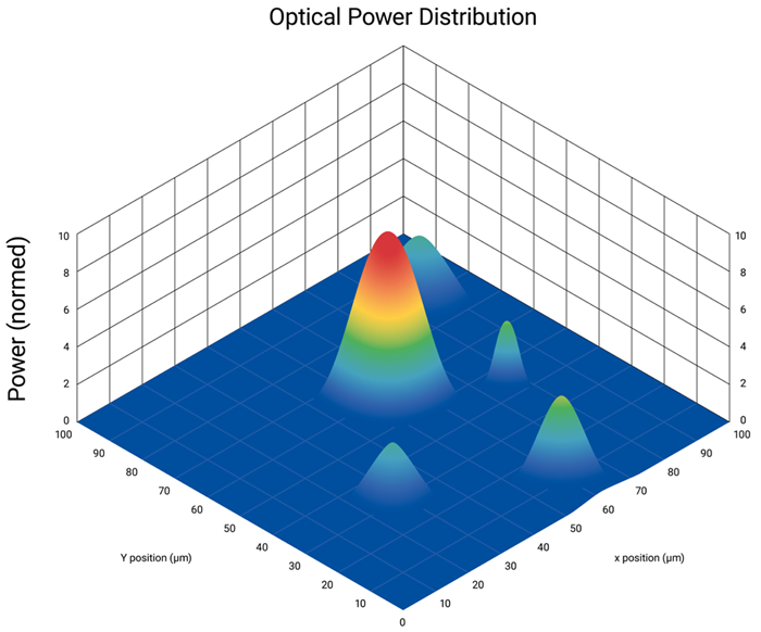
Figure 2. Power distribution of an optical component shows multiple peaks. Modern algorithms and precision mechanics can help determine the main mode and find the exact peak quickly. Image Credit: PI (Physik Instrumente) LP
Advanced Alignment Algorithms and Fast Precision Mechanics
A revolutionary combination of advanced algorithms and quick mechanisms, such as PI's award-winning Fast Multichannel Photonics Alignment solutions (FMPA), has significantly increased throughput.
FMPA optimizes coupling between photonic elements across channels, inputs, outputs, and DOFs, even when these independent variables influence each other. To achieve this, the system incorporates functionalities such as rapid first-light detection, a vibrationless areal scan, and an innovative parallel gradient search capable of real-time, multivariate tracking optimization. Another advancement is the PILightning First Light Detection algorithm that can reduce time to find first light by orders of magnitude, especially in dual-sided alignment applications.
Previous approaches required coupling to be tuned sequentially, looping back and forth and readjusting at each axis to gradually establish a consensus. This took a long time, sometimes several minutes, and had a substantial influence on costs, efficiency, and scalability.
In comparison, FMPA can make all of these changes in a single step using a simple set of commands that take only seconds to execute.
Because the alignments are executed concurrently, the optimization time is substantially independent of the number of alignments. This considerable reduction in alignment time, generally two orders of magnitude, dramatically lowers costs, making operations like probing SiPh wafers commercially viable.
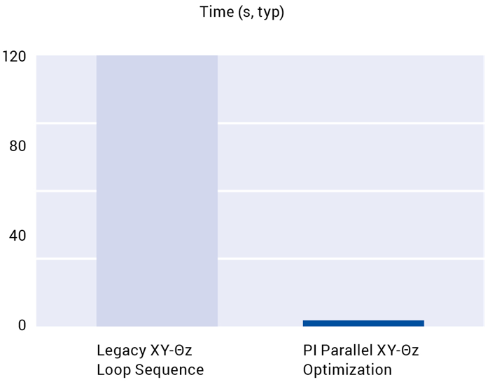
Figure 3. Alignment speed is crucial in reducing production costs. Image Credit: PI (Physik Instrumente) LP
Download the full article now to learn more
References
- Taylor, P. (2024). Data Created Worldwide 2010-2025 . Statista. Statista. Available at: https://www.statista.com/statistics/871513/worldwide-data-created/.
Acknowledgments
Produced using materials originally written by Scott Jordan and Stefan Vordran from Physik Instrumente.