Nearly a decade ago, Physik Instrumente (PI) introduced its Fast Multichannel Photonics Alignment (FMPA) technology, combining parallel-kinematic motion systems with advanced parallel alignment algorithms. By enabling multiple optical alignment processes to run simultaneously, FMPA dramatically reduced alignment times while improving production throughput. The technology quickly earned industry recognition, including an R&D 100 Award and a Lightwave Innovation Award, for its innovative approach to high-speed photonics alignment.
Examples of the processes include:
- For alignments in multiple degrees of freedom. A ubiquitous example in Silicon Photonics (SiP) is any fiber array unit (FAU), where alignment motions in θZ (common notation for rotation about the optical axis) lead to dealignment in XY. Previously, any corrective motion in θZ required pausing and realigning in XY, making array alignment a time-consuming process. FMPA’s parallel alignment ability enables complete device alignment in a single rapid step, as compensating for the geometric errors due to θZ motions occurs in parallel with them.
- For optical elements whose positional optimization depends on other elements. This includes waveguide structures with inputs, outputs, and channels that can interact, such as short waveguides with inputs and outputs that “steer” each other. Additional examples include lenses or diffractive elements in imaging or resonator assemblies with interrelated mutual positions. By performing these optimizations in a single step, FMPA achieves global optimization that is frequently 100 times quicker than previously feasible.
This significant reduction in global alignment time significantly impacts test and assembly prices for photonic products. Industry literature confirms that alignment has the biggest impact, overall, on product price.1
Since alignment must be conducted multiple times across various process stages in the test and photonics device assembly, FMPA’s substantial reduction in process time is highly leveraged.
Silicon Photonics Manufacturing Is Following the Same Path as the Early Semiconductor Industry
Today's silicon photonics industry is in many ways where the semiconductor industry stood in the mid-1980s. Back then, building a semiconductor fab involved far more than placing purchase orders for production equipment. Many of the required manufacturing tools simply did not exist as commercial products. Industry leaders such as IBM developed highly customized production equipment, often working with dedicated systems integrators or internal engineering teams to create the automation they needed.
The photonics industry is experiencing a similar transition today.
As demand for silicon photonics manufacturing, optical assembly, and wafer-level testing continues to accelerate, commercially available production tools have struggled to keep pace. Many existing automation platforms are still based on concepts developed during the fiber-optic telecommunications boom of the late 1990s and early 2000s, when long-haul optical networking was the industry's primary growth driver.
Today's market is fundamentally different.
Silicon photonics now serves a rapidly expanding range of applications, including AI data centers, co-packaged optics, quantum technologies, LiDAR, biomedical imaging, sensing, high-speed communications, and advanced computing. These diverse markets require far greater flexibility, precision, and scalability than legacy photonics production equipment was designed to deliver.
For years, memories of the telecom downturn discouraged significant investment in new photonics manufacturing platforms. As a result, many device manufacturers and contract manufacturers have continued to design and build custom automation systems in-house - much like semiconductor pioneers did decades ago.
That is finally beginning to change. Companies such as FormFactor, with its advanced Cascade wafer probing systems, and Tegema, with integrated photonics assembly platforms, are introducing new production solutions tailored to modern photonics manufacturing. At the same time, motion-control specialists and automation suppliers are enabling standardized, high-precision building blocks for alignment, testing, packaging, and assembly.
As the silicon photonics industry moves from research to high-volume production, it is increasingly following the same evolution the semiconductor industry experienced four decades ago: transitioning from custom-built manufacturing equipment toward standardized, scalable production platforms capable of supporting industrial-scale manufacturing.
Silicon Photonics Production Example
Because the identities of most PI customers are confidential, this representative manufacturer will be referred to as Substantial Photonic Company (SPC).
SPC manufactures optical networking hardware based on photonic integrated circuits. Its devices combine photonic chips with multiple optical input/output channels, lasers, photodiodes, fiber arrays, and other optical components. After wafer-level probing, the photonic chips are singulated and transferred to the packaging process2. A critical step in this workflow is the precise alignment and attachment of fiber arrays to the individual chips.
As discussed previously, the limited availability of suitable commercial photonics production equipment led SPC to develop its own manufacturing tools. This approach also enabled the company to integrate advanced automated alignment technology, including PI’s Fast Multichannel Photonics Alignment (FMPA) solution.
In this application, as in most silicon photonics alignment processes, the primary optimization parameter is the optical power transmitted through multiple channels of the device. The alignment system must identify the position that maximizes coupling efficiency across the complete channel array while meeting production requirements for speed, repeatability, and yield.
During photonic device testing and assembly, measurement data are typically transmitted to the PI motion controller using one of three methods:
Optical Monitor Tap
An optical monitor tap provides direct access to a portion of the light passing through a device or optical channel. This signal may also be used for other measurements during testing and assembly, including spectroscopy and optical power characterization.
In these applications, a high-bandwidth optical power meter can feed an analog signal directly to the ultrafast analog inputs of the PI alignment controller. The power meter must therefore provide a sufficiently fast analog output.
Optical power meters designed specifically for automated photonics alignment, such as PI’s F-712.PM1, provide a rapid logarithmic output. This eliminates the need for auto-ranging, which would otherwise interrupt or slow the alignment process. The logarithmic response also provides a wide, multi-decade dynamic range, allowing the system to capture and optimize signals ranging from very low coupling levels to peak optical throughput.
Photocurrent Tap
Some photonic devices incorporate an on-chip photodiode or similar detector that measures the optical power passing through a channel. The resulting photocurrent can be routed outside the device and used as the optimization signal.
A high-bandwidth transimpedance amplifier converts the photocurrent into a voltage that the FMPA controller can rapidly evaluate during alignment. The external photodiode input available on the F-712.PM1 provides this capability while retaining the benefits of a logarithmic response and broad dynamic range.
This approach is particularly useful when direct optical access is limited or when the device already includes integrated monitoring photodiodes.
RSSI Port
In some devices, optical signal strength can only be accessed through a Received Signal Strength Indicator, or RSSI, interface. The RSSI value is typically queried through a digital communication protocol such as I²C or SPI.
In a production photonics alignment workstation, a microcontroller can repeatedly poll the RSSI port and convert each digital reading into an analog voltage. That voltage is then supplied to the FMPA controller as the optimization signal.
A simple microcontroller platform can perform these queries rapidly in a continuous loop, allowing the automated alignment system to maximize optical coupling even when the device does not provide a direct analog optical-power output.
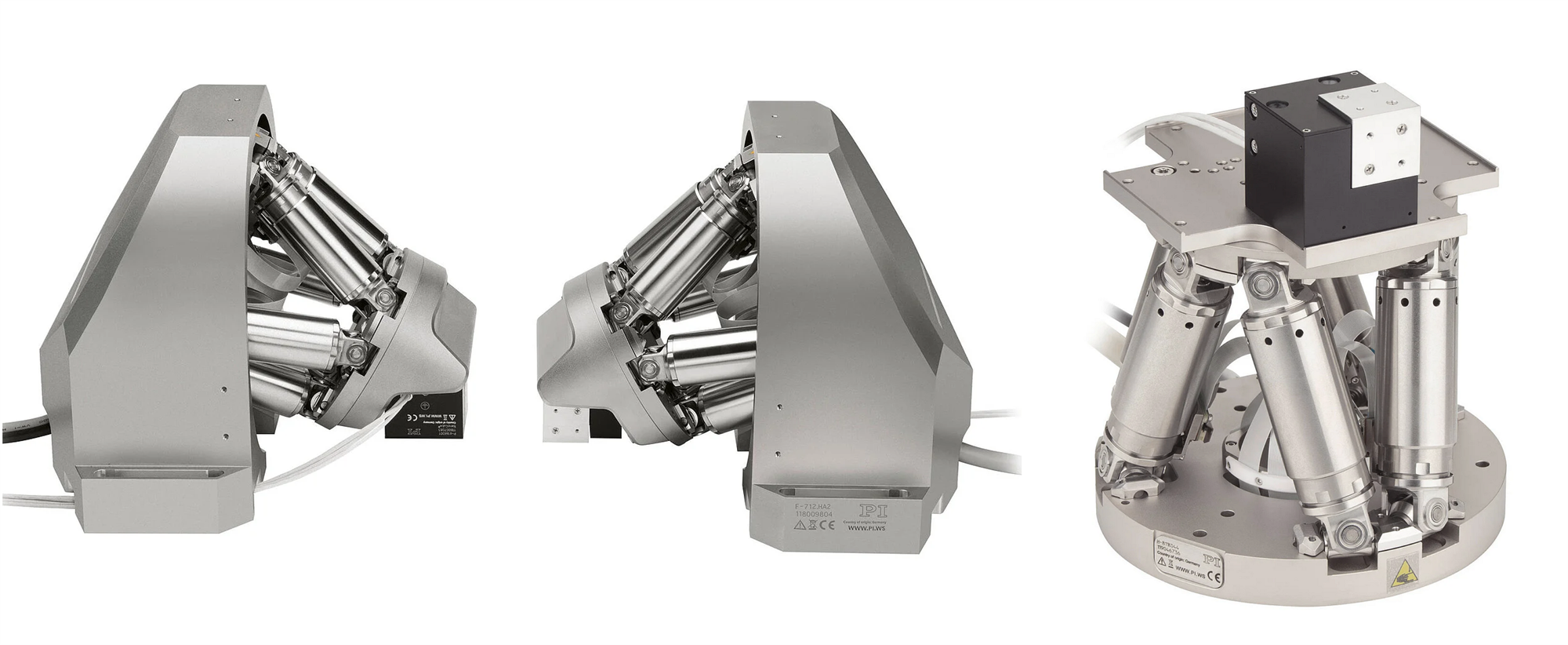
Figure 1. The F-713 Fast Multi-Channel Alignment 6-axis Micro-Robot is available in upright and low-profile configurations, both single- and dual-sided . This assembly combines a Nanocube® fast, high-resolution closed-loop 3-DOF piezo nano-scanner and a long-travel, 6-DOF hexapod driven by brushless DC servo-motors. These Image Credit: PI (Physik Instrumente) LP
SPC uses a combination of these signal-acquisition methods across its production applications. For FAU attachment, the company selected PI’s F-712.HU1 Fast Multichannel Photonics Alignment system (Figure 1) and deployed more than three dozen units at its contract manufacturing facility. The automated alignment and attachment of the fiber array to the silicon photonic chip proceeds as follows:
- The FAU is brought into close proximity with the silicon photonic chip.
Because SPC’s manufacturing process is tightly controlled, the initial Z-axis gap is repeatable to within a few micrometers. Other manufacturers may need to establish or verify this gap before alignment begins. Several techniques can be used for this purpose:
- Machine vision: Advances in compact USB cameras have made machine vision far more accessible, often reducing the need for expensive industrial cameras and dedicated frame grabbers. Open-source vision libraries such as OpenCV and intelligent camera platforms such as OpenMV can simplify tasks including device-presence verification, edge detection, angular alignment, and Z-gap measurement.
- Contact sensing: FMPA systems can be equipped with optional force sensors offering milligram-level sensitivity. These sensors allow the system to detect initial contact between components and establish the Z = 0 reference position. The motion system can then retract by a defined distance to create the required assembly gap.
- Optical geometry: A series of area scans can be performed at progressively increasing Z positions to measure beam divergence and calculate the absolute separation between the fiber array and the photonic chip. This can be a cost-effective approach because PI FMPA systems include integrated area-scan functionality that is also commonly used for device qualification.
- Beam-waist detection: In applications involving a focused beam waist, such as lensed-fiber alignment, the FMPA system can perform a Z-axis gradient search to rapidly identify the optimal axial position. A simultaneous XY gradient search maintains peak optical coupling when the mechanical and optical axes are not perfectly parallel.
- Proximity sensing: When the device geometry permits, a proximity sensor such as a capacitive probe can directly measure the separation between components, allowing the required Z-axis gap to be established quickly and accurately.
- In SPC’s application, the F-712.PM1 power meter’s six- to seven-decade dynamic range usually enables immediate detection of first light in the first channel of the FAU. When first light is not detected immediately, the NanoCube® can perform an area scan across its full 100 × 100 µm range, typically in 300 ms or less. Area scanning is an integrated controller command and includes runtime options such as automatic Gaussian fitting. The hexapod provides nearly identical scan and alignment functionality, but over ranges extending from micrometers to millimeters. The NanoCube® and hexapod can also scan simultaneously, enabling rapid searches across ranges of tens of millimeters while maintaining submicrometer scan resolution.
- Once first light is detected in the first channel, the NanoCube® performs a continuous gradient search to optimize coupling and maintain lock-on in real time.
-
Because the hexapod can rotate around any user-defined point in space, its pivot point is positioned near the optical axis of the first channel. The hexapod then performs a θZ optimization using the second channel4. The NanoCube’s continuous XY lock-on automatically compensates for small errors in the defined rotational center, allowing the translational and rotational alignment processes to run in parallel. This simultaneous optimization is a key advantage of FMPA.
For devices that also require tip-and-tilt correction, θX and θY optimizations can be performed concurrently.
The total time for steps 1-4 is around one second. Glue is subsequently applied; the XY tracking corrects any disturbance from this and accommodates drift during the early phases of epoxy polymerization. System options can include provisions for light-curtain and other safety interlocks, and soft limits are a standard feature for implementing forbidden zones to avoid collisions.
References and Notes
- Barwicz, T. et al. (2017). Automated High-Throughput Assembly for Photonic Packaging. Photonics Summit, Cadence, 2017. Available at: https://www.cadence.com/content/dam/cadence-www/global/en_US/documents/company/Events/summits/photonics/fortier-2017.pdf and Fuchs, E.R.H., et al. (2006). Process-based cost modeling of photonics manufacture: The cost competitiveness of monolithic integration of a 1550-nm DFB laser and an electroabsorptive modulator on an InP platform. Journal of Lightwave Technology, 24(8), pp.3175–3186. DOI:10.1109/jlt.2006.875961. https://ieeexplore.ieee.org/document/1667840.
- FormFactor Inc. (2019). Autonomous Silicon Photonics Measurement Assistant | FormFactor. YouTube. Available at: https://www.youtube.com/watch?v=izM33rfVVc4.
- In principle, FMPA can optimize virtually any hill-shaped figure-of-merit that can be measured or calculated with sufficient speed, including things like extinction ratio for polarization-sensitive alignments, calculations of image sharpness for imaging optic assembly, or calculations of beam quality for laser assembly. In addition, PI controllers allow virtually any fast, measured quantity to be used as a servo input, allowing automatic positioning to achieve a desired set-point.
- The identical approach is used for devices with a U-shaped loop-back channel, as often found for facilitating assembly alignment.

This information has been sourced, reviewed and adapted from materials provided by PI (Physik Instrumente) LP.
For more information on this source, please visit PI (Physik Instrumente) LP.