The Mönch 4107 is a cathodoluminescence detector for STEM that has been built from the ground up to realize unparalleled signal-to-noise ratio and spectral resolution. It is used by demanding researchers who are keen on measuring simultaneously ultra-high-resolution images and hyperspectral maps of individual quantum dots, nanoparticles, or atomic defects. The design behind the Mönch 4107 has a solid publication track record, which includes reports on nano-plasmonics, simultaneous measurements of cathodoluminescence and EELS, non-linear spectroscopy of individual quantum wells, quantum nano-optics and more.
When obtaining a cathodoluminescence map in a STEM, it is crucial that one reaches the preferred signal-to-noise ratio in the least amount of time possible, so that images can be generated with a large number of pixels. Yet, one can only accomplish ultrahigh resolution with weak probe currents, resulting in weak cathodoluminescence emission. Consequently, the ideal cathodoluminescence detector is bound to accomplish the impossible: it should gather photons over an extensive solid angle and fit in the small gap between a sample and the pole pieces of the STEM; it should also preserve spectral resolution, brightness, and collection efficiency across large scanning areas.
The Attolight Mönch 4107 realizes all this. First, its collection optics is crafted by Attolight engineers with maximum care to attain unparalleled curvature radius and miniaturization level; it is so thin that it can be housed in most aberration corrected or analytical STEMs available in the market, while maintaining sufficient degrees of freedom and stiffness to allow for flawless sub-micrometer alignment of the mirror while installed in the STEM.
Then, the Mönch 4107 gathers and couples cathodoluminescence directly into a fiber bundle and carefully preserves the intensity of the signal throughout a spectrometer, so that constant spectral resolution is realized. Lastly, an ultrafast EMCCD camera measures the signal and produces huge hyperspectral maps in seconds. Data can be directly attained and visualized in user’s favorite acquisition software in parallel with other methods (EELS, EDS, etc.).
The Mönch 4107 is not only another add-on. It is a solution produced by a company that designs electron microscopes and has years of expertise in spectroscopy and optics. Attolight took all the know-how it assimilated designing and manufacturing dedicated cathodoluminescence scanning electron microscopes and used it to develop STEMs. The Mönch 4107 includes a proprietary actuated collection mirror for rapid and perfect optical alignment, a scientific grade high speed camera for fast hyperspectral data acquisition, a fiber coupled spectrometer for high resolution spectral analysis, as well as a hyperspectral optimized scanning module for optimal control of the STEM beam.
Key Benefits
- Brightness conservation from emission to detection
- Constant spectral resolution (no trade-off with intensity)
- Sub-micrometer precision mirror actuators with three degrees of freedom to realize perfect collection efficiency at any position on the sample
- Entire sample area can be tested
- Fits within a 2 mm gap between the sample and the pole piece
- Retractable mirror
- Ultrafast cameras and scanning unit for millisecond hyperspectral imaging in the visible, UV, and NIR
- Compatible with Gatan Digital Micrograph
- Compatible with a majority of STEMs methods, such as BF, diffraction, HAADF, EELS (detector inserted) or EDS, tomography (detector retracted)
Applications
- Investigation of advanced materials, such as: Nitrides (InGaN, GaN, AlGaN, …); III-V (GaP, InP, GaAs, …); II–VI (CdTe, ZnO, …)
- Wide band-gap materials (AlN, diamond, BN)
- Confined structures or heterostructures morphology to their optical properties
- Compositional inhomogeneities in compound materials (for instance, Indium clustering in InGaN)
- Plasmonics
- Defects (threading dislocations, vacancies, stacking vaults, …)
Product Specifications
Measurements Mode
- Hyperspectral mapping of cathodoluminescence
Light Optics
- Proprietary reflective mirror
- Collection optics optimized for transition from 200 nm to 1.7 µm
- Optical coupler for fiber bundle
- Fiber bundle to decouple the light optics from the spectral detection and reduce vibrations
- All numerical apertures match each other so as to keep brightness throughout the device
- Possibility to couple the cathodoluminescence output to a user optical set-up (for example, interferometer, light injector, etc.)
- Possibility to quickly exchange the fiber bundle to adapt to specific user needs (for example light injection or interferometry…)
Light detectors
- High speed EMCCD camera for UV-Visible or high speed CCD camera for UV-NIR
- Dispersive spectrometer with two imaging exits (320 mm focal length) and a 3-grating turret (gratings to be indicated by the customer at time of order)
- InGaAs linear array for NIR (optional)
Micro-Positioning System
- Three degrees of freedom for arbitrary movement of the mirror relatively to the sample
- Travel range: ±150 µm (Z), 3 mm (X), 100 mm (Y)
- Automated retractable mirror
- Smallest increment: 50 nm
- Touch security to avoid damaging the pole piece or sample holder
- Repeatability (full travel range): 1 µm
System Control
- External scanning card with: four inputs (12 bits) for additional single channel detectors (PMTs, …); two outputs for controlling the STEM scan (X and Y); 1 output for blanking the STEM beam
- Fastest measurement speed: 900 Hz (18 s for a 128 × 128 map)
- Acquisition and visualization module for Gatan Digital Micrograph
- Control software compatible with Windows® 7, 64 bit
Installation Requirements
- STEM with a minimum of 2.5 mm gap between the specimen and the pole piece (the total gap for a symmetric pole piece must be 5 mm). Smaller design on request
- Sample holder with less than 300 µm between the sample surface and its holder (many commercial sample holders can be adapted by Attolight to attain theses specifications)
Selected Applications
Nanophotonics
Imaging GaN/AlN nanodisks
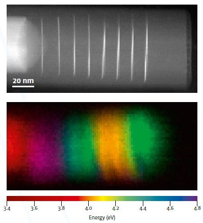
Lifetime Measurements Well below the Optical Diffraction Limit
S. Meuret et al., ACS Photonics, 3, 1157–1163 (2016).
Material Science
Imaging UV defects in hexagonal boron nitride
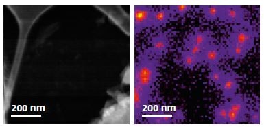
Bright UV Single Photon Emission at Point Defects in h-BN
R. Bourrellier et al. Nano Letters, 16, 4317–4321 (2016).
CL of biological samples
Vesicle classification with functionalized nanodiamonds
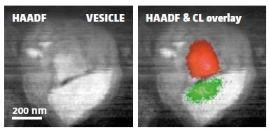
Simultaneous cathodoluminescence and electron microscopy cytometry of cellular vesicles labeled with fluorescent nanodiamonds.
S. Nagarajan, C. Pioche-Durieu, L. H. G. Tizei, C.-Y. Fang, J.-R. Bertrand, E. Le Cam, H.-C. Chang, F. Treussart, and M. Kociak Nanoscale, 8, 11588 (2016).
Nanophotonics
Imaging plasmon modes in metal nanoparticles
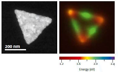
Extinction and Scattering Properties of High-Order Surface Plasmon Modes in Silver Nanoparticles Probed by Combined Spatially Resolved Electron Energy Loss Spectroscopy and Cathodoluminescence
N. Kawasaki et al. ACS Photonics, 3, 1654–1661 (2016).