An ultra-flat and pristine gold surface is provided by template-stripped gold chips for research applications, such as biosensor development, scanning electron microscope (SEM) and atomic force microscopy (AFM) and analyses of self-assembled monolayers.
The gold chips are produced by coating the flattest prime-grade silicon wafers available or a newly split mica, without an adhesion layer.
Following this, glass chips measuring 1 x 1 cm2 are epoxy-glued to the gold surface. The gold surface employed by the users is the one that comes in contact with the mica or silicon substrate, and hence, it is ultra-flat and also protected from the air until it is ready to be used.
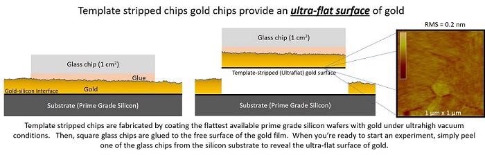
Image Credit: Platypus Technologies LLC
Features and Benefits
- RMS roughness that approaches atomic flatness
- Ready to use: Chips do not need cleaning and thus prevent the need for costly cleaning equipment or toxic cleaning solutions
- Uncontaminated surface: Gold is protected from the air until it is removed from the template, offering a pristine surface that does not contain organics and other kinds of atmospheric contaminants
- Convenient: With numerous chips for each template, clean, fresh and ultra-flat chips can be prepared within seconds before the next experiment
Ordering Information
All chips are delivered in aluminosilicate glass, 1 x 1 cm. But users can contact Platypus Technologies for alternative chip dimensions.
Comparison with Standard Gold
Ultra-flat and standard gold surfaces were examined by AFM across a randomly chosen 1-µm2 area to evaluate roughness.
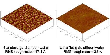
Image Credit: Platypus Technologies LLC
Surface Orientation
The ultra-flat gold films from Platypus Technologies have an even (111) orientation covering the whole surface area of the chip.
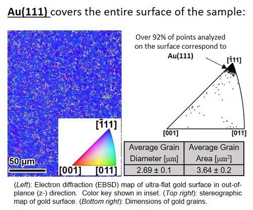
Image Credit: Platypus Technologies LLC
Applications
Ultra-flat gold surfaces allow high resolution characterization of self-assembled monolayers (SAM) and single molecules through scanning tunneling microscopy (STM) or AFM. Ultra-flat gold surfaces are perfect for use in single-molecule imaging, self-assembly, DNA origami, nano-photonics and nano-contact printing.
Ultra-flat gold is used in the following studies:
- C. Ciano et al. “Phonon-Polaritons in flakes of h-BN” Appl. Phys. Lett., 2018.
- X. Jia et al. “Surface modes of periodic nanopatch metasurface” Optics Express, 2018.
- H. Wang et al. “Electron tunneling across plasmonic junctions” Phys. Chem., 2017.
- K. Jimenez et al. “Electronic Conductance through DNA molecules” J. Phys. Chem. A, 2017.
- M. Sajfutdinow et al. “Patterning of self-assembled monolayer (SAM)” Nanoscale, 2017.
- G. Akselrod et al. “Enhancement in plasmonic nanoantennas” Nature Photonics, 2014.
- T. Lee et al. “Construction of RNA-Quantum Dot for Nanoscale Biomemory” ACS Nano, 2015.