The JEOL JSM-IT810 series is a revolutionary, ultra-high-resolution Field Emission Scanning Electron Microscope (FE-SEM). This advanced instrument combines exceptional versatility, high spatial resolution, and user-friendly automation, making it a powerful tool for high-resolution imaging and analysis at the nanoscale.
Smart-Flexible-Powerful
Smart
The JEOL IT810 series of Schottky Field Emission SEMs has an embedded JEOL Energy Dispersive X-ray Spectrometer (EDS), designed to streamline operations and enhance workflow efficiency. The powerful software, with its ultra-high resolution and elegant functionality, enables seamless data acquisition, from initial observation to elemental analysis and reporting.
This device is powered by the JEOL NEOENGINE® electron beam control system, which, along with advanced auto functions, enables fast transitions between high-resolution imaging and high-current analyses without sacrificing performance. Sophisticated algorithms work in real time to automatically align the beam, optimize electron lenses, and correct focus, brightness, and astigmatism. With JEOL’s Live EDS analysis, users can even directly monitor a specimen's chemical composition during imaging.
The JEOL SEM integrates optical imaging, navigation, and EDS Live analysis with a simple one-click operation.
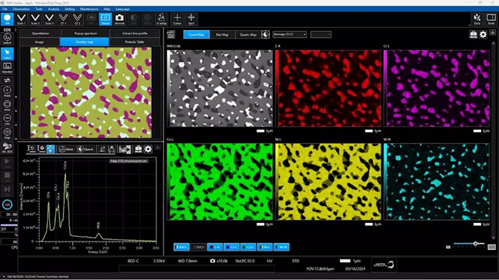
Image Credit: JEOL USA, Inc.
Flexible
The JSM-IT810 series is equipped with a large specimen chamber that can accommodate a wide variety of detectors simultaneously, including multiple EDS, WDS, EBSD, STEM, BSE, and CL detectors. The system's GatherX windowless EDS detector offers higher sensitivity for low-energy X-ray detection (down to Li). At the same time, the unique Soft X-ray Emission Spectrometer (SXES) allows for efficient, parallel collection of very low-energy X-rays to provide unprecedented chemical state analysis.
Powerful
As JEOL’s flagship Field Emission SEM, the IT810 is exceptionally powerful, with a magnification range of up to 2,000,000× and an accelerating voltage range of 0.01 to 30 kV.
With these magnifications and voltages, the IT810 is able to produce stunningly detailed images of nanostructures and perform a comprehensive analysis. Overall, this highly versatile and easy-to-use SEM delivers the next level of analytical intelligence.
Innovative No-code Automation
The software interface is intuitive and customizable, simplifying high throughput in routine observation and analysis. It features new no-code automated workflows, included with every IT810 series microscope.
Key Features
- Aperture Angle Control Lens (ACL) for superb resolution at any kV or probe current
- High spatial resolution imaging and analysis of nanostructures
- Smile View Lab for data management and report generation
- The Beam Deceleration (BD) mode minimizes the effects of lens aberrations.
- Large specimen chamber with multiple ports
- NEOENGINE – intelligent automated electron beam control
- The system features advanced auto functions that automatically handle key tasks like beam alignment, focus, and stigmation
- In-lens field emission gun
- The system's versatile electromagnetic/electrostatic hybrid lens design provides outstanding performance for both imaging and analysis
- Live Analysis with integrated JEOL EDS elemental screening
- Montage imaging features are standard
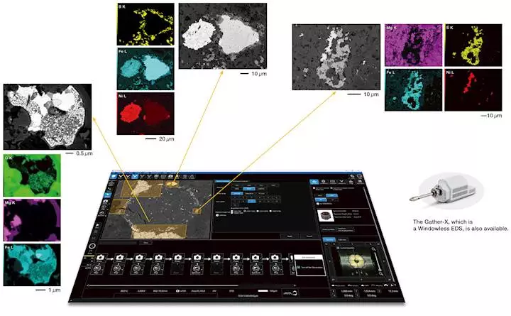
Automatic Observation and Analysis Function "Neo Action"
The user can easily automate both SEM observation and EDS analysis by setting the analysis conditions and selecting the areas the user wants to measure.
Sample: Chondrules in chondrite Julesberg (L3.6) Landing Voltage: 5 kV. Image Credit: JEOL USA, Inc.
SEM Automatic Adjustment Package
The optional SEM Automatic Adjustment Package uses a dedicated sample to perform magnification calibration, beam alignment, and EDS energy calibration. These regular checks ensure the equipment remains in excellent condition.
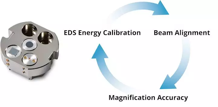
Image Credit: JEOL USA, Inc.
Live-3D Function
With the multi-functional, semiconductor-type BSE detector, users can create a live 3D reconstruction of the sample's surface and instantly check its topology.
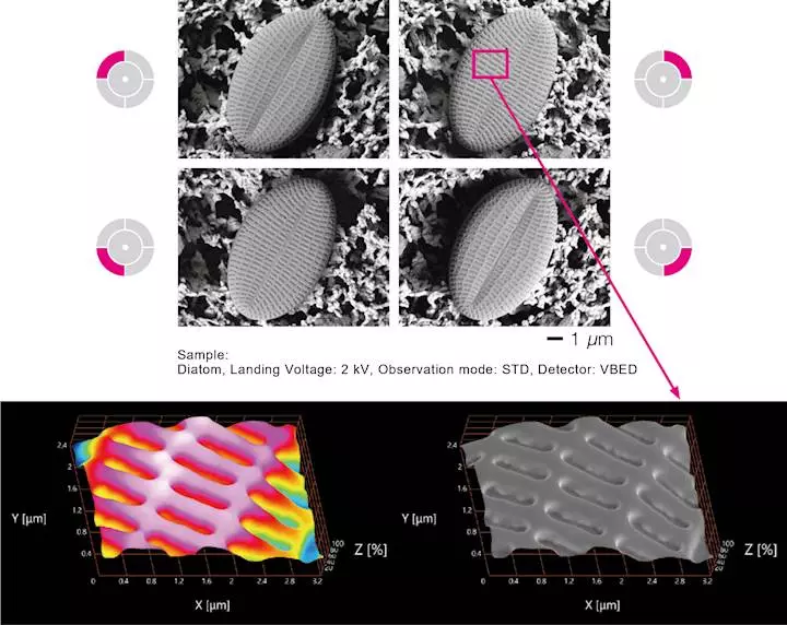
Image Credit: JEOL USA, Inc.
EDS Integration
This next-generation system adeptly integrates SEM imaging with EDS elemental analysis, removing the barriers between them. A user can now select and reserve various analysis methods, such as point, area, MAP, and line, directly on the observation screen, allowing the user to begin analysis immediately.
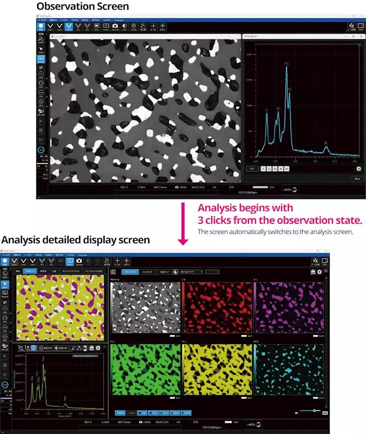
Image Credit: JEOL USA, Inc.