Semiconductor research and production go hand in hand with silicon wafers, and one of their most critical properties is surface roughness. Even tiny irregularities can have a major impact on device performance. Excessive roughness, for instance, can degrade key electrical characteristics by reducing the mobility of electrons and holes, ultimately compromising the efficiency and reliability of the final device.
This effect extends far beyond electrical performance, influencing every stage of semiconductor manufacturing, from adhesion and photolithography to overall device reliability. A rough wafer scatters charge carriers, driving up resistance and cutting efficiency, which might impair high-performance CPUs, GPUs, and memory chips. It also downgrades thin-film adhesion, photolithography precision, and even optical properties in LEDs and solar cells. Worse, roughness can trigger cracks and defects in the material, reducing yield and reliability.
Therefore, manufacturers of semiconductors must constantly monitor the roughness of silicon wafers, a parameter defined as the root mean square of height deviations from the mean at each point, which is typically in the subnanometer (angstrom) range. Atomic force microscopy is the natural choice for this task, but traditional dynamic mode has long frustrated the community with its slow speed. This challenge is now solved with Nanosurf’s WaveMode, available on the DriveAFM and the industrial Alphacen 300 Drive systems. WaveMode is up to 15 times faster than conventional dynamic mode, setting a new benchmark for subnanometer roughness measurements and making DriveAFM the future standard in semiconductor metrology.
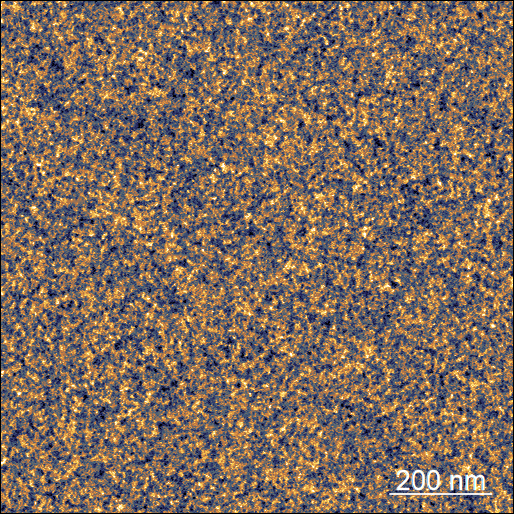
Surface of a silicon wafer imaged with DriveAFM using WaveMode at 15Hz of line rate. The whole image took less than 34 seconds to be acquired. Image Credit: Nanosurf AG
WaveMode is possible thanks to the CleanDrive technology, consisting of a second laser which excites the cantilever off-resonance phototermically; unlike other implementations of off-resonance modes, WaveMode has the advantage that it does neither need nor rely on subtraction of any parasitic background. The photothermal excitation allows to overcome the f/Q limit typical of the dynamic mode. “Adding the Fast Scanning option, an additional piezo able to rapidly track the surface, enables faster response times and significantly higher scanning speeds.”, adds Carolina Paba, Application Scientist at Nanosurf. In the production line of a semiconductor factory, this means higher throughput.
Another key feature of WaveMode is its ability to precisely control the tip-sample interaction, minimizing the risk of damage to both the surface and the probe tip. Preserving the tip condition allows repeated measurements over extended periods without frequent tip replacement, reducing operational costs. As direct consequence, WaveMode ensures high reproducibility of results. “What is important for semiconductor applications is that repeated measurements across a wafer deliver consistent roughness values, even when the probe moves to distant points. With WaveMode, we have demonstrated that the tip remains stable, ensuring that roughness measurements do not drift over time. This means reproducible results under the same conditions, even during extensive repetitions,” comments Paba. In our dataset, collected over 9 consecutive days, the distribution of measured roughness remains consistent, and this confirms that the tip quality is preserved from start to finish and delivering low noise datasets.
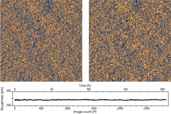
Time-series of surface roughness measurements of a silicon wafer using WaveMode. Images in the top row show images at the beginning of the series and after nearly 9 days. The graph below shows the roughness determined from each image of the series. Image Credit: Nanosurf AG
With respect to traditional AFM modes, WaveMode is exceptionally easy to use. In dynamic mode, the interaction regime, attractive or repulsive, depends on parameters such as oscillation amplitude and setpoint, which define the force between the tip and the sample. Small changes in these settings can easily shift the system from one regime to the other, making the interaction less stable. WaveMode can be configured in just a few clicks through a simple, intuitive procedure. It also provides visual feedback on the applied force, giving users immediate control and confidence during measurements.