Graphene is a single atomic sheet of carbon atoms in the arrangement found in graphite. The fact that it is thermodynamically stable as a single layer allows the exploitation of its unique electron transport properties. In particular, the two-dimensional electronic properties of graphene presents the potential for it to function as a conductor, a transistor, a quantum dot, a molecular switch, or other devices. The lateral confinement of the layer, however, is key to causing these behaviors to be expressed. It is also very important in researching these phenomena to have the ability to control, based on top-down designs, where the patterning is done in relationship to probes and external connections.
Current Techniques Available for Pattering Graphene
At the present time patterning of graphene is accomplished by techniques such as STM or electron beam lithography, but these suffer from throughput and process control constraints which limit the achievable repeatability of the structures. Therefore it would be attractive to directly pattern the necessary structures with good control. In addition, a complete solution also requires high resolution imaging in order to place the cuts and verify the results.
Imaging and Machining Graphene Using The ORION® PLUS from Carl Zeiss
The ORION® PLUS makes it possible both to image and machine graphene in one seamless operation. The high resolution of the microscope – a world record value for surface imaging at 0.25 nm – combined with its extreme surface sensitivity allows the imaging of small graphene features with single monolayer detection. There is in addition a benefit with the helium ion beam in that it can gently machine graphene. A low sputter yield, estimated to be between 0.006 and 0.02 carbon atoms per helium ion, depending on sample thickness and substrate type, means that imaging can be done safely in a lower dose regime while nano-scale milling can be done at higher dose. By toggling the ion optics configuration between these two modes one can carry out the entire device formation process: identifying the area of interest, defining the machining geometries, making the cuts and inspecting the result.
Figure 1 demonstrates both the high surface sensitivity for imaging graphene and the speed control for material removal. The image reveals a lot of surface detail on the sample. A 500 nm area in the center of this image was subjected to a higher dose of helium ions at 38keV. This facilitated the removal of a small amount of material from the surface. Inspection shows how the topography was made flat but without significant milling into the surface.
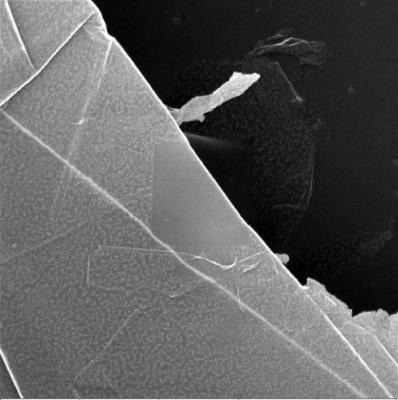
Figure 1. ORION® PLUS image of graphene layers (thickness not determined) showing surface modification. A small ion dose was applied to the outlined area. A thin surface layer could selectively be removed.
Figure 2 shows a complete breakthrough milling operation. In this case a much larger dose was applied to a 100nm square area, making a cleanly machined feature all the way through the layers. This type of machining is not possible with an SEM, because there is no sputtering. It is also beyond the reach of traditional gallium FIB, which would create too much damage and would also introduce metallic contaminants into the feature. Since the sputter yield is so low, it is possible to obtain a high signal to noise image at an ion dose two orders of magnitude below what is required to remove a single monolayer of graphene – meaning that imaging is non-destructive to the sample. We have demonstrated by this process the ability to create a 20nm wide ribbon in a single layer of graphene – a requirement for testing two-dimensional semiconducting properties in this material.
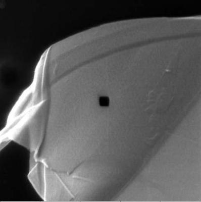
Figure 2. ORION® PLUS image of graphene layers showing ion milling. The small square area in the center is a 100nm box machined completely through the material. The edge acuity of the box demonstrates the excellent achievable resolution which can be achieved for patterning.
Application
High spatial resolution patterning of graphene layers for research and prototyping in semiconductor or material science fields. This is for the creation of devices of nanometer dimensions that will exhibit new useful properties due to electron confinement.
ORION® PLUS Capabilities
High resolution and surface sensitivity to image graphene sheets; the ability to select either imaging or machining modes; non-contaminating operation.

This information has been sourced, reviewed and adapted from materials provided by Carl Zeiss.
For more information on this source, please visit Carl Zeiss.