Since the first Nano Imprint Lithography (NIL) publications, interest in the technology has grown rapidly - starting with the scientific community and then moving to industrial sectors like integrated optics, sensors and micro fluidics.
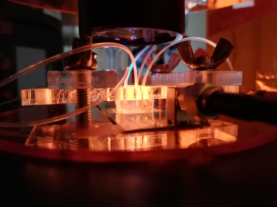
Image Credit: Shutterstock/Molpid
NIL offers several technical advantages with respect to resolution, overlay accuracy, and tool design. In addition to creating high resolution features in the nanometer range, NIL can also be employed for replicating much larger features. Presently, NIL is utilized in optical applications for the production of optical elements with feature sizes in the sub-millimeter range. With the ever increasing demand for higher integration of functionality, combined with the need to reduce structure sizes at acceptable costs, traditional lithographic techniques are fast approaching their limits. NIL is a competitive candidate for Next Generation Lithography (NGL) due to its advantages in resolution and cost effectiveness.
The potential of this technology has been acknowledged by leading experts. Subsequently, it has been added to the International Technology Roadmap for Semiconductors (ITRS) as a potential NGL solution for microelectronics at the 32 nm node and beyond.
EVG offers solutions within the three main areas of Nanoimprint Lithography (NIL):
- Hot Embossing (HE),
- UV-based Nanoimprint Lithography (UV-NIL) and
- Micro Contact Printing (µ-CP).
What is UV-Nanoimprint Lithography?
In UV-NIL, a substrate is spin coated or drop dispensed with a UV-curable monomer or oligomer. Imprinting is carried out with a transparent template (quartz glass or soft working stamps) and the imprinted structures are cured by UV-light exposure which cross-links the resist. Subsequently the template is released from the imprinted substrate. The use of quartz glass stamps is regarded as hard UV-NIL whereas the use of soft working stamps refers to soft UV-NIL.
Full Field Large Area UV-Nanoimprinting
A dispensed UV curable material is imprinted at a pre-programmed contact force with UV transparent stamps. UV irradiation cures the polymer. Both soft and hard stamps can be used on EVG systems. UV transparent hard stamps are usually made of quartz glass (SiO2). Soft stamps are similar to those used in micro contact printing (e.g. PDMS) where the stamp is mounted on a thin, conformal or a thick, rigid backplane. Soft stamps are typically used for large area imprinting applications. The release process after curing is supported by an anti sticking layer as well as by a non-parallel release mechanism.
Step and Repeat Large Area UV-Nanoimprinting
The EVG770 NIL Stepper is designed for step and repeat UV-NIL processes and is compatible for 100 mm to 300 mm wafers. The special features of the EVG770 include a dual-stage alignment approach and the capability to imprint in a lower pressure environment (patent pending technology), which enables greater pattern fidelity compared to other technical solutions which imprint at ambient pressure. The step and repeat NIL system targets sub-25 nm overlay alignment accuracy and has already demonstrated a lithography resolution in the sub-20 nm range.
Principles of UV-Nanoimprint Lithography
.jpg)
Source: EVG
.jpg)
Five layer photonic crystal in Si/SiO2 utilizing UV-NIL, alignment < 100 nm. Source: EVG
.jpg)
Soft UV-NIL imprinted 50 nm pillars. Source: EVG
.jpg)
NMOSFET on SOI. Source EVG, Courtesy of AMO GmbH
.jpg)
70/130 nm lines/space. Source EVG, Courtesy of LTM/LETI
Nanoimprint Lithography Systems for UV-Nanoimprint Lithography
EVG®510UV-NIL/HE Hot Embossing System
The EVG510UV-NIL can be configured as a manual UV-NIL and/or Hot Embossing system for R&D processes. The field proven EVG510UV-NIL system architecture provides the best capabilities for large area applications requiring vacuum imprinting.
.jpg)
The EVG510UV-NIL UV-NIL and/or Hot Embossing system. Source: EVG.
EVG®620 UV-NIL System
The EVG620NIL system allows for imprint processes with stamps and substrates from small chip size pieces up to 150 mm in diameter. Configurations for nanotechnology applications can include release mechanisms for stamps in addition to programmable high and low contact force. Uniform contact force for high yield, large area printing is provided by EVG's proprietary chuck design which supports both soft and hard stamps. In addition to that, the EVG620 can be configured as a multiple use system in combination with optical lithography and micro contact printing.
.jpg)
The EVG®620 UV-NIL system. Source: EVG.
EVG®6200 UV-NIL System
The EVG6200 Infinity is the culmination of EVG's new aligner technology roadmap and provides the same capabilities as the EVG620. A variety of stamps and substrates sizes, from 75 mm to 200 mm, is possible on the EVG6200 Infinity for nanoimprint lithography applications.
.jpg)
The EVG®6200 UV-NIL system. Source: EVG.
IQ®Aligner UV-NIL System
The IQ Aligner allows for imprint processes with stamps and wafers from 150 mm to 300 mm diameter. Configurations for nanotechnology applications can include stamp release mechanisms and programmable contact force capability. A temperature controlled chuck for large substrates provides unmatched stamp to substrate overlay accuracy. Uniform contact force for high yield large area printing is provided by EVG's proprietary chuck design which supports both soft and hard stamps. The IQ Aligner can be used for micromolding processes for the fabrication of optical elements as well as for nanoimprint lithography.
.jpg)
The IQ®Aligner UV-NIL system. Source: EVG.
EVG®770 UV-NIL Stepper
The special features of EVG's EVG770 NIL stepper include a dual-stage alignment approach in lower pressure environments. This step and repeat UV-NIL system enhances pattern transfer fidelity compared to other technical solution which operate only in ambient pressure. The EVG770 targets sub-25 nm overlay alignment accuracy and a lithography resolution in the sub-30 nm range. The special features of the EVG770 can be summarized as follows:
- Vacuum imprinting for superior pattern fidelity
- Dual stage alignment approach (first print and fine alignment)
- Spun on polymer layer utilizes industry standard coating techniques
- Chuck system with edge handling
- Active optical sensors to bring stamp and wafer into perfect parallelism for contactless wedge
- compensation and adjustment of the separation gap during alignment
.jpg)
The EVG®770 UV-NIL stepper. Source: EVG.
Soft and Working Stamp Fabrication
Due to the thickness variation of standard substrates, the use of a rigid quartz stamp for UV-NIL is limited to an effective patternable area of approximately 25 mm x 25 mm. Therefore, in order to pattern larger areas (e.g. 300 mm wafers), a step and repeat process must be employed. However, EVG, with its NILCom partners, have made recent advances in soft UV-NIL which allow for imprinting of the entire substrate surface in a single step.
This method is preferred in several applications where:
- a non-polar surface has to be patterned
- a continuous pattern without any stitching errors is required (e.g. waveguides); and
- either relaxed specifications on alignment accuracy are allowable or the imprint is a first-print application.
.jpg)
Source: EVG.
EVG has demonstrated full-field, soft UV-NIL with this technology down to 50 nm resolution. Our soft stamp technology offers reduced cost-of-ownership and processing benefits over competing methods due to the following reasons:
- they are fabricated on standard mask aligners using fast, UV curing techniques (~20x times faster than PDMS stamps);
- they have inherently low surface energy and thus do not require anti-stiction coatings;
- they can be used to make submasters allowing flexibility in the master stamp fabrication;
- the working stamp can be used to make several imprints (>2000 demonstrated in microlens molding).
Additionally, initial tests show that these same working stamp materials used for UV-NIL can also be employed for hot embossing into spun-on polymers. This novel application provides several advantages including more facile de-embossing, especially during automated processing.
This information has been sourced, reviewed and adapted from materials provided by EV Group.
For more information on this source, please visit EV Group.