There has been a considerable expansion in optical metrology techniques and applications during the decade that has passed since the publication of the first edition of the Optics Encyclopedia. Much of this has been driven by new enabling technologies, from high speed cameras to advanced lasers. Increasing capital equipment investment in metrology has been another driver, fulfilling the demands of high value-added products from semiconductors to precision-engineered automotive parts. This article on optical metrology provides examples of these trends.
Distance and Displacement Measurements
Fiber Sensor for Ultra-precision Positioning
The fiber itself is used as a transducer in many fiber optic sensing systems (see the section titled “Fiber Sensors,” in ADVANCES IN OPTICAL METROLOGY, the section titled “Optical Fiber Sensors,” in FIBER OPTICS, and in the section titled “Fiber Interferometers,” in INTERFEROMETRY in The Optics Encyclopedia), but there are also advantages to distribution and light collection systems that measure distances in free space. There is a long history of measurements of distance or change of distance (displacement) using fiber optics in partial or complete replacement of traditional bulk optics such as prisms, mirrors, and lenses. [1] Ease of setup and alignment, and, often, the ability to multiplex sensing technologies to multiple sensing areas are the advantages of fiber optics. Sensing methods differ from coherent interferometry to intensity-modulated laser radar. [2, 3]
A new generation of devices that combine compact size with installation flexibility is represented by high-accuracy, interferometric fiber-based distance sensors. These new sensors allow object position and high-precision (pm) stage motion over macroscopic ranges (mm) with unmatched performance requirements. For example, advanced photolithography systems need zero heat dissipation in the sensing elements, position monitoring of projection optics and other critical subsystems with subnanometer drift over many hours, as well as extraordinary reliability over several years to prevent system down time. Flexibility in sensor location is important, as is compact sensor size and insensitivity to electromagnetic interference.
An approach to meeting the demanding goals of photolithography systems separates a high-cost, complex metrology subsystem from a collection of simple, high-reliability sensors embedded within limited access areas. The heat-generating components are shifted to locations outside the thermally controlled structure of the photolithography system, and unlike traditional capacitance gages or encoders that must be energized to function, the sensors themselves are passive. Figure 1 shows one such architecture using the coupled- cavity principle, employing a spectrally broad light source to enable remote phase modulation of Fizeau-type fiber sensors having a fixed standoff. [4] The details of a design for a passive sensor are provided in Figure 2. Practically, there may be dozens of such reference cavities and sensors for environmental compensation, all controlled by the same control box. In certain configurations, the method of exact fractions and multiple wavelength methods allow the establishment of the absolute position of the target relative to the measurement datum. [5] Table 1 sums up the performance characteristics of a system for advanced positioning applications. [6, 7] The drift specification of 1 nmday−1 and the exceptionally low noise of 0.014 nm-Hz−1/2 are particularly remarkable.
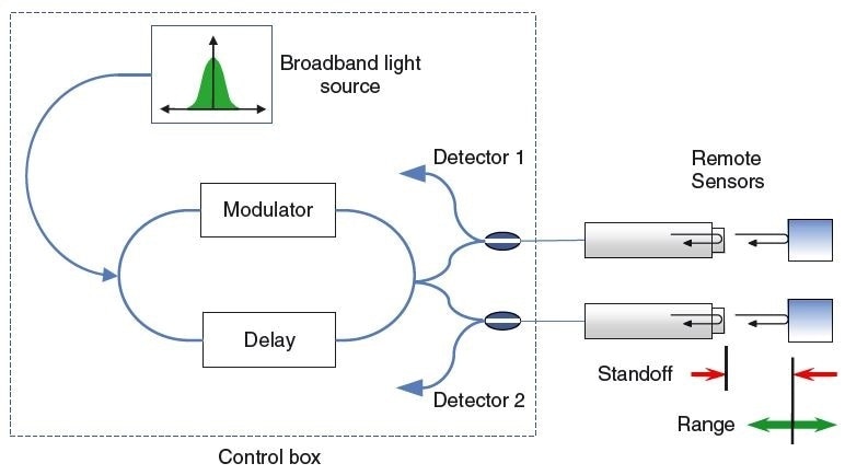
Figure 1. Principle of multiplexed remote fiber distance measurement
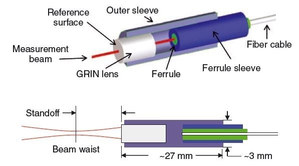
Figure 2. Details of position sensor construction that leverages the reliability of telecommunication components and construction techniques
Table 1. Performance characteristics of the fiber interferometer [6]
| Parameter |
Value |
| Number of channels |
64 |
| Measurement range |
1.2 mm |
| Standoff |
3.5 mm |
| Repeatability (1 kHz) |
0.5 nm |
| Bandwidth |
100 kHz |
| Noise (3σ) |
0.014 nm-Hz-1/2 |
| Drift |
1 nm/day-1 |
| Linearity |
2 nm |
Heterodyne Optical Encoders
Stage positioning in photolithography systems is one of the most demanding applications of optical metrology. [1] Previously, free-space, plane mirror displacement interferometers have served this application well (see the section titled “Multiaxis Laser Heterodyne Stage Metrology,” in ADVANCES IN OPTICAL METROLOGY in The Optics Encyclopedia). The growing demands of ever-shrinking features on semiconductor wafers have went beyond the ability of these free-space systems to accommodate the unavoidable disturbances caused by air flow and environmental sources of ambiguity (see the section titled “Environmental Compensation,” in ADVANCES IN OPTICAL METROLOGY in The Optics Encyclopedia). Approaches to overcome these problems using dispersion interferometry or other techniques have been superseded by a transition to optical encoder technology, particularly, to heterodyne interferometric methods. These methods depend on highly precise 2D grating structures which are fundamental to the moving parts of the lithography system.
The transition to grating-based displacement monitoring over free-space interferometry has driven encoder technology far beyond conventional designs and capabilities (see Figure 7 in the section titled “Optical Encoders,” in ADVANCES IN OPTICAL METROLOGY in The Optics Encyclopedia). Instead of being the low-cost option, encoders are presently the premium solution. The incorporation of heterodyne techniques, along with unique optical designs that enable these techniques, has been the major upgrade to the technology.
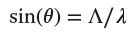
Figure 3 represents one such design, illustrating a configuration that enables for measurement of the vertical (z) motion and lateral (x) motion of the grating in accordance with the encoder assembly [8]. The system consists of two interferometers working together to deliver this information. In the figure, the source light, arriving from the right, is separated into two beams and each are further split into orthogonally polarized reference and measurement beams (see the section titled “Heterodyne Laser Sources and Detectors,” in ADVANCES IN OPTICAL METROLOGY in The Optics Encyclopedia). A frequency difference of the reference and measurement beams corresponds to the polarization-encoded frequency split of the source light. The measurement beams propagate to the grating and get diffracted there. Some of the diffracted beams are blocked as shown in the figure, whereas others are returned to the grating in retroreflection. The returned beams again diffract to the beam- splitting prism, where they combine with the reference beams and propagate to two detectors. Polarizers combine the two polarizations, leading to heterodyne beat signals at the difference frequency.
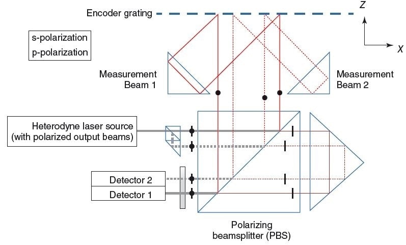
Figure 3. Heterodyne encoder for simultaneous measurement of in- plane (x) and out-of-plane (z) motions
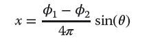
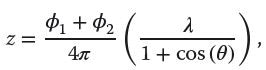
The phases Φ1, Φ2 of each of the two detected signals is sensitive to both x- and z-axis motions. To calculate the motions independently, these formulas are formulated
 |
(1) |
 |
(2) |
where λ is the illumination wavelength and
 |
(3) |
is the sine of the first-order diffraction angle. The basic geometry readily extends to three dimensions.
The Figure 3 configuration has a disadvantage in the out-of-plane motions that result in a beam shear, which can be a problem for large displacements in the z-direction. The use of plane-mirror interferometers operating in a Littrow configuration are alternative geometries. [9–11] The double-pass geometry of Figure 4 employs complementary incident angles to compensate for beam sheer at the detector. [12]
Heterodyne encoders are now well recognized in advanced stage metrology systems and maintain the subnanometer noise level of free-space interferometry with much reduced sensitivity to turbulence and airflow. This comes at a price of a much more extensive calibration of the encoder grating and other geometric factors associated with Abbe offsets and compound motions.
Figure 4. Double-pass encoder with beam sheer compensation [12]
Surface Form and Optical Testing
Form Metrology in Challenging Environments
The issue of unexpected mechanical motions and turbulent airflow during data acquisition has long been a disadvantage of surface-measuring laser Fizeau interferometry (see the section titled “Optical Flat and Laser Fizeau Interferometers,” in ADVANCES IN OPTICAL METROLOGY in The Optics Encyclopedia). Over the past 10 years, there have been remarkable advances in single camera frame instantaneous interferometry, to match the multiframe data acquisition characteristic of conventional phase shifting interferometry (PSI, see the section titled “Phase Estimation for Surface Profiling,” in ADVANCES IN OPTICALMETROLOGY in The Optics Encyclopedia). These techniques depend on the introduction of phase shifts spatially instead of over time, which in turn requires encoding of the reference and measurement beams of the interferometer so that their relative phase can be manipulated [13]. This technique offers environmental insensitivity, and the possibility of capturing dynamically changing events with high-speed camera shuttering.
A number of configurations of single-frame interferometry use multiple phase shifted images using polarization encoding of the measurement and reference paths and either multiple cameras [14] or a single camera with subfields [15]. The technology enables a form of homodyne detection without the necessity for a temporal phase shift. The invention of the pixilated polarizer mask for 2D camera arrays [16, 17] has been an important development in this type of single-frame interferometry. A configuration using a Twyman– Green interferometer [17] is shown in Figure 5. The simultaneous acquisition of four interwoven images with 90° phase shifts removes the need for mechanicalor optical-phase shifting methods. This is an important advantage for production-floor applications and measurements where the object and the interferometer are essentially on separate supporting structures, as in the case, for instance, in the testing of large astronomical mirrors.
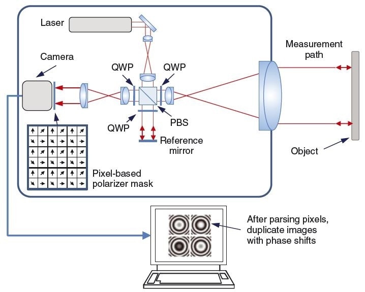
Figure 5. Single camera-frame homodyne interferometry using a pizelated mask
The method has been widely developed, with variants available for Fizeau systems [18, 19] and 3D microscopy [20]. A limitation of the method is the need for a polarized system, which complicates the optical design and necessitates calibration for systematic errors [21].
An alternative to the polarized interferometry is a traditional method occasionally known as carrier fringe interferometry [22–24]. In this method, an intentional tilt angle between the reference and measurement wavefronts leads to a dense pattern of numerous interference fringes, equivalent to an electronicholographic image of the object surface (see the section titled “Holographic Shape Recording,” in Advances in Optical Metrology in The Optics Encyclopedia). Fourier analysis of these fringes enables the extraction of interference phase without the need for polarization of the reference and measurement beams, as illustrated in Figure 6. As with polarized single-frame techniques, the carrier fringe method comes at the price of a more intricate optical design that must be enhanced and calibrated to tolerate the difference in ray paths within the interferometer system between the interfering beams [25]. Figure 7 shows one application of a high-speed carrier fringe interferometer, for the mapping and visualization of heated airflow [26].
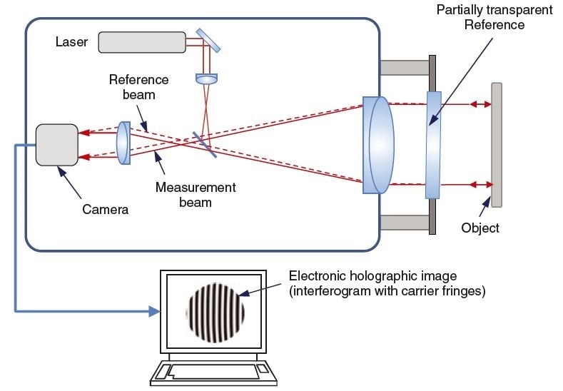
Figure 6. Single-frame dynamic interferometry using the carrier fringe technique and Fourier analysis.
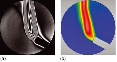
Figure 7. Single-frame capture of dynamic thermal gradients viewed (a) as interference fringes and (b) as a processed 3D map. These results are viewed live through high-speed data processing to facilitate interpretation of rapidly changing, dynamic events
Deflectometry
Interferometry offers surface height precision with some parallels in metrology, but there is a cost and simplicity benefit to basic shape sensors based on the geometry of light propagation rather than interference. Moiré and structured light techniques, for instance, are quick and effective means for measuring objects ranging from car bodies to electronic interconnects on semiconductor wafers and packages (see the section titled “Structured Light,” in Advances in Optical Metrology in The Optics Encyclopedia) [27].
For smooth, mirror-like surfaces, several methods detect surface slopes by the law of reflection (see the section titled “Geometric slope testing,” in Advances in Optical Metrology in The Optics Encyclopedia). In contrast to projected fringe or Moiré approaches, no patterns are imaged onto the object surface; instead, the metrology principle depends on the specular reflection of light rays from a test surface that is effectively a component of the collective optical imaging system. Advanced versions of this general idea include the Hartmann and other screen test, commonly involving an electronic camera and a screen or lenslet array to outline and image narrow ray bundles [28].
A progressively popular geometric slope testing technique today in some sense is a Hartmann test in reverse [29]: in place of a screen or lenslet array at the imaging pupil, the test surface reflects blurred light from a patterned screen into a small imaging pupil of a camera. Slope mapping happens via the trajectories of the chief rays of the system, with camera pixels mapped to positions on the object surface, and the recorded intensities for each pixel mapped through surface slopes to coordinates on the object. The technology is called the Software Configurable Optical Test System [29], the Fringe Reflection method [30], or more generally, Deflectometry [31].
Figure 8 shows a regular configuration using a programmable pattern screen for deflectometry. The pattern may be a scanned line [29], a sequence of points, or a phase modulated sinusoidal pattern [32]. The surface is in focus, which means that the screen pattern is deliberately blurred. However, a sinusoidal fringe stays sinusoidal even when not in focus, and in any case the imaging pupil is deliberately small so as to extend the depth of focus while isolating the chief rays. Modulation of the pattern, using, for instance, PSI techniques (see the section titled “Phase Estimation for Surface Profiling,” in Advances in Optical Metrology in The Optics Encyclopedia).
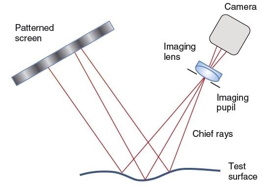
Figure 8. Principle of phasemeasuring deflectometry. Surface points map directly to pixels on the camera using the imaging lens. Modulation of the sinusoidal intensity pattern enhances determination of the location of the origin on the screen of each ray.
A number of deflectometry systems have remarkably simple and straightforward hardware – in certain cases, the patterned object is a conventional laptop computer screen, and the integrated camera serves as the detector. A cellphone, likewise, can be configured for deflectometry. Limitations of deflectometry are mainly related to the ambiguity of measurement, which stems from the need for widespread calibration to translate image points and intensities first into surface slopes at precisely demarcated locations on the test surface and then into an overall height map using slope integration. Regardless of impressive sensitivity on the nanometer scale to high-spatial frequency surface features, preliminary versions of the technology were recognized as lacking in form accuracy compared to interferometry. Direct first applications of deflectometry include free-form surfaces such as progressive eyeglass lenses, which are complex test objects for interferometers, but less challenging requirements for surface form uncertainty than precision optics [33]. Extra applications include machined metal parts with modest tolerances.
Progress in calibration has revealed that deflectometric methods may have the potential to contend interferometry for high-precision measurements for specular surfaces, particularly for mid-spatial frequency measurements of free-forms and aspheres [31]. Universal optimization techniques involve numerous images of artifacts and determination of all applicable calibration factors in a single step [34]. New applications range from large astronomical telescope optics to X-ray mirrors [35], with fascinating agreement with stylus, interferometric, and long-trace profiler measurements. Deflectometry is one of numerous examples of where advanced computing power, in this case for multivariable optimization and calibration, has enabled outstanding new applications for a renowned concept in optical metrology.
Microscopic Surface Structure
Focus Sensing and Confocal Microscopy
At high magnifications, the imaging properties of optical systems rely greatly on what may be generally termed as focus effects. In a conventional microscope, the focus effect exhibits itself as blurred or sharp images based on the location of the object surface with regard to the microscope objective. It is natural and intuitive to consider using this phenomenon for surface metrology.
Focus sensitive measurements, like microscopy, are old techniques but automated systems for 3D surface topography analysis are comparatively recent. The concept is direct: First establish a quantitative measure of focus, then scan through a range of focus positions, and lastly examine the focus properties as a function of scan to determine height over a range of surface positions [36].
A good feature of this technology is that it requires only a few changes to current digital microscopes that use electronic cameras and software-controllable system focus. Nevertheless, latest developments have focused on dedicated systems enhanced for metrology, along with advanced data processing and wide-ranging applications development. Benefits of focus variation include the ability to measure steeply-sloped surfaces, including those well outside the capture range for specular reflection in epi illumination. The operating principle accommodates a wide variety of imaging modes, with some of the most stimulating configurations employing source light in a darkfield configuration.
Restrictions of focus variation include some major issues, such as the need for intensity contrast in the surface image as a mechanism for establishing surface height. Therefore, the technique is best adapted to modestly rough or diffusely reflecting surfaces. The height precision is ideal for high-NA objectives, which limit applications that need a large field of view with low uncertainty in the surface topography result. Other restrictions include the possibility of confusion with some curved surface features and transparent films that can create ghost images of high focus contrast. Lastly, as the technique requires comparing imaging pixels, the lateral sampling should be extremely high compared to the optical resolution to exploit the available lateral resolution. Notwithstanding these restrictions, the method has found many exciting applications in 3D imaging for precision manufacturing, owing to its robustness and versatility.
The reliance on lateral pixel comparisons surface texture characteristic of focus variation instruments can be avoided by projecting a modulated pattern onto the object, in a manner similar to fringe projection [37] but relying on the focus effect in place of conventional triangulation (see the section titled “Structured Light,” in Advances in Optical Metrology in The Optics Encyclopedia). Theoretically, the structured illumination microscopy or SIM realizes optical sectioning in a conventional wide-field microscope by projecting a grid pattern onto the object [38]. The contrast of the grid pattern relies on the focus position, as shown in Figure. 9.
The sensitivity of the contrast to focus relies on the depth of focus and on the spatial frequency of the grid pattern. An extra hardware change to allow for modulating the grid pattern enhances the system’s ability to detect small variations in contrast, for instance, by using a conventional phase-shifting method at different height positions [40].
A continuous oscillation of the grid pattern during a concurrent continuous height scan allows for emulation of low-coherence interferometry signals (see the section titled “Scanning White-light Interferometry,” in Advances in Optical Metrology in The Optics Encyclopedia), including the use of data-processing algorithms and methods [39]. An advantage over interferometry, however, is that the equivalent wavelength and contrast envelope in SIM can be adjusted by selecting the grid pattern, scanning rate, and modulation rate. A supplementary flexibility afforded by spatial light modulator technology is to control the grid pattern frequency, shape, and modulation dynamically based on the object shape and structure (Figure 10) [39].
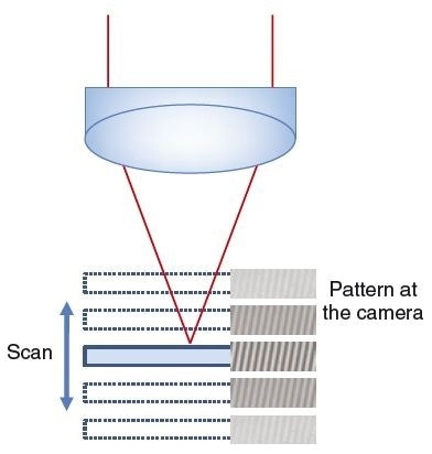
Figure 9. Structured light 3D microscopy [39]
![Example structured illumination microscopy (SIM) signal using the technique of Ref. [39] to emulate the signal from an interference microscope, but with adjustable equivalent wavelength and fringe contrast envelope. Here, the equivalent wavelength is 8 µm.](https://www.azonano.com/images/Article_Images/ImageForArticle_4821_447892717561458348945.jpg)
Figure 10. Example structured illumination microscopy (SIM) signal using the technique of Ref. [39] to emulate the signal from an interference microscope, but with adjustable equivalent wavelength and fringe contrast envelope. Here, the equivalent wavelength is 8 μm.
A major and important technology for improving the focus effect depends on physical or virtual apertures to more precisely define the position of ideal focus. Confocal microscopes section 3D structures into planar images, rejecting undesirable light and in certain cases refining lateral resolution by isolating and aperturing the point spread function (see the section titled “Confocal Microscopy,” in Microscopy in The Optics Encyclopedia). A number of configurations fall within the category of confocal microscopy, based on the implementation [41]. Historically, the key field of application of the confocal microscope has been for confocal fluorescence microscopy of biological specimens; however, in recent times, there have been increasing applications in industrial and high-technology 3D imaging for metrology.
A traditional method to confocal microscopy uses a rotating Nipkow disk [42] to facilitate forming an image quickly from a moving array of pinholes. In the system of Figure 11, the same disk is used for both the illumination and imaging pinhole, using an optical isolator (not shown) to eliminate direct reflections from the surface of the disk [43]. This arrangement functions with a high intensity, diffuse illumination, and the image reconstruction is sufficiently fast to allow for a real-time, visual interpretation. More recent approaches to confocal imaging depend on lenslet arrays to enhance light efficiency, with adequate point density to eliminate the need for the Nipkow disk [44]. Another method uses a programmable illumination of small pinholes or thin lines, but the imaging filtering is performed by the detection array itself, and the programmable illumination sweeps the object electro-optically [45].
In laser scanning units, the high spatial coherence of the laser removes the need for an illumination aperture (see the section titled “Laser-scanning Microscopy,” in MICROSCOPY in The Optics Encyclopedia). A galvanometric system consecutively scans over an area of object surface points, and a pinhole-imaging aperture spatially filters the returned light, which isolates the height position of the highest intensity transmission. After the conclusion of a full-field scan of the laser, a mechanical scanner moves the system to the subsequent imaging plane, building up in this way a complete 3D image. Laser scanning confocals are of specific interest in the life sciences, as they enable tomographic imaging of turbid media with fluorescent markers under strong laser light [46].
A progressively popular configuration is the chromatic confocal system, wherein the height scan characteristic of traditional image sectioning confocal is substituted by wavelength coding of the surface height planes [47]. This can be unexpectedly easy to realize, at least as a proof of concept, by taking any confocal system and using optics with high longitudinal chromatic aberration. Under these conditions, the position of best focus is governed by the wavelength. A spectroscopic analysis identifies these best-focus image planes, removing the need for a height scan. The principle is prevalent for single- point probes and for systems that use lateral xy scanning to build up complete images, but is also viable with a Nipkow disk arrangement [48].
As is the case for all focus-based systems, the noise level of confocal microscopy trends toward improved performance with higher NA. Figure 12 reveals this trend. The dependence on NA is a strength as well as limitation: Confocal microscopes can obtain data at very high speeds at low magnification, but at the expense of a higher noise level. For objectives higher than 0.75 NA, the noise approaches 1 nm, surpassing interferometric methods.
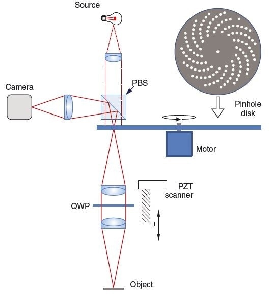
Figure 11. Nipkow disk confocal
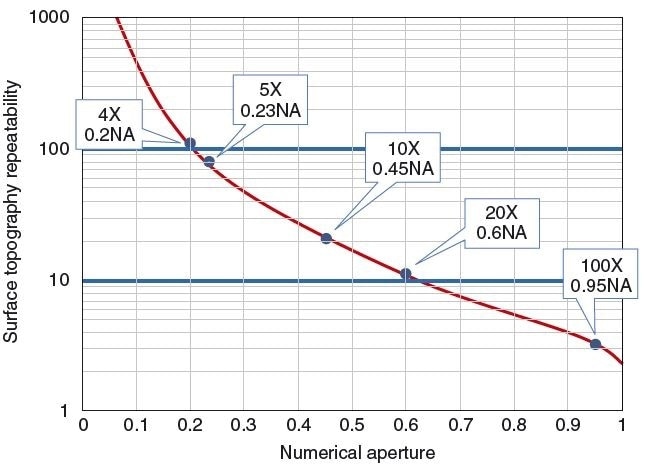
Figure 12. Typical single-measurement surface topography repeatability at visible wavelengths for focus-based instruments, including confocal, structured illumination, and focus-sensing microscopy. The curve may be higher or lower on this graph depending on the specific hardware and data processing
Advances in Interference Microscopy
Competitive 3D technologies such as confocal and focus sensing have raised the standard for interference microscopes for slope acceptance, ease of use, and flexibility. These competitive pressures, along with a quickly growing necessity for areal surface topography measurement in wide areas of precision manufacturing and high-technology component development [49, 50], provide a motivation for continuous enhancement in optical interferometry.
Presently, the dominant interferometric method for topography measurement over small fields of view is coherence scanning interferometry (CSI) (see the section titled “Scanning White-light Interferometry,” in Advances in Optical Metrology in The Optics Encyclopedia). CSI microscopy has a leading role to play in the measurement of waviness, form, and roughness on surface areas from 0.05 to 5 mm in diameter, with a height ambiguity that in certain cases is well below 1 nm [51, 52]. Traditional restrictions have included the local slope of mirror-like surfaces, which in principle should be sufficiently small to allow for specular reflection of the illumination into the capture range of the objective. However, it is in principle possible to measure further than this limit by banking on scattered light.
Significant improvements in signal detection sensitivity at present allow for measurements of polished surfaces beyond the traditional slope limits. Figure 13(a) illustrates an example of a polymer microlens measured with a 50× Mirau objective with a numerical aperture of 0.55 and a corresponding specular limit of 33°. This figure illustrates meaningful topography data with measured slopes up to 60°. Figure 13(b) illustrates a retroflector array created in uncoated mirror-finish polymer, with slopes outside the specular limit. Data coverage is complete on the diagonal sides [53].
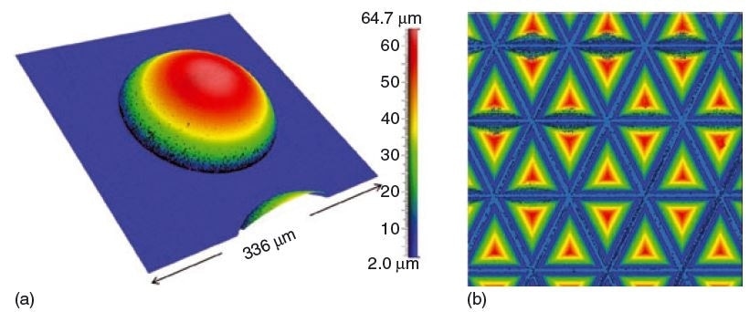
Figure 13. CSI measurements of objects having steep slopes. (a) Microlens. (b) Array of pyramidal structures in a light diffuser.
Demands for high precision over large areas for both surface form and texture have boosted the development of new interference objective designs to expand the field of view of conventional CSI microscopes. The most typical configurations for high-magnification microscope interference objectives are of the Mirau and Michelson designs (see the section titled “Interference Microscopy,” in Advances in Optical Metrology in The Optics Encyclopedia). Below 10× magnifications, equivalent to a field size of about 2 mm, all commercial interference objectives have been of the Michelson type, in which a beam splitter directs a portion of the illumination to a reference mirror orthogonal to the test surface. The large prism beam splitter and orthogonal reference path have been a hindrance to extending the field of view of Michelson objectives over 10 mm. As a consequence, large-field CSI instruments use a dedicated Twyman Green geometry instead of the conventional microscope system [54, 55]. A newly introduced wide-field, equal-path interference objective uses a beam splitter and partially transmissive reference mirror coaxially, as illustrated in Figure 14 [56]. The partially transmitting reference and beam splitter plates are angles so as to reject undesirable reflections. This design allows for considerably larger fields of view, up to 60 mm diagonal with a 0.5× de-magnifying objective, using a conventional microscope system. The same design allows for wide fields of up to 20 mm in a parfocal turret-mountable objective – considered to be an impractical configuration using Michelson objectives [57].
![Wide field of view (60 mm diagonal) 3D metrology microscope objective. [56]](https://www.azonano.com/images/Article_Images/ImageForArticle_4821_4478927176160888395.jpg)
Figure 14. Wide field of view (60 mm diagonal) 3D metrology microscope objective. [56]
More computing power has also enabled new applications for interference microscopy built on modeling of the interference signal. The model-based method starts with a more full and accurate characterization of the interferometer and how the light interacts with the object surface [58]. Then, the inverse problem is solved to discover parameters such as film thickness by comparing experimental and theoretical signals (or the Fourier Transforms) over a range of possible surface structures [59]. The first and most well-documented application of model-based CSI has been 3D profiling of transparent film thickness and topography, as shown in Figure 15. This is a capability hard to match in any other tool – reflectometry may provide film thickness profiles but not topography, while tactile gages offer topography over films but without film thickness. These same methods enable techniques for parameter metrology of optically unresolved surface structures [60], a capability formerly restricted to scatterometry.
Figure 15. Map of photoresist thickness near a transistor gate on a TFT LCD panel using model-based analysis. The horseshoe-shaped trench is nominally 400-nm thick and 5-μm wide. [59]
Optical Metrology for the Life Sciences
Optical Coherence Tomography
Closely associated with CSI (see the section titled “Scanning White-light Interferometry,” in Advances in Optical Metrology in The Optics Encyclopedia) but following an autonomous development, optical coherence tomography (OCT) as a life science instrument started in the late 1980s as a broadband, near-infrared (0.8–1.3 μm wavelength), single measurement point probe for the examination of the eye [61]. In the configuration of Figure 16, the beam paths are guided by optical fiber, constant with the ideal case of a spectrally broadband yet spatially coherent light source [62]. Early systems were of the time-domain (TD) type, meaning that the reference arm of the interferometer was mechanically articulated to produce a time-dependent depth scan of the translucent object (see the section titled “Optical Coherence Microscopy,” in Microscopy in The Optics Encyclopedia). Light scattered from the interfaces between differing materials results in numerous signals or echos as shown in Figure 16. A 3D image is built up from a sequence of single-point axial A scans, using a lexicon borrowed from ultrasonic imaging. Moving the probe beam laterally produces a cross section (referred to as a B-scan) of depth versus lateral position [63], while a raster-scan motion produces a complete tomographic 3D image.
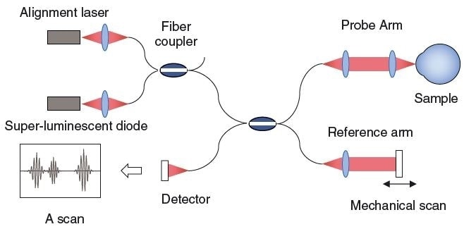
Figure 16. Classic time-domain optical coherence tomography (TD- OCT) system for single-point axial A scans. [62]
The original TD-OCT method is slow for mechanical reasons, given the need to physically displace the reference or an equivalent technique such as a fiber stretcher in the reference arm. More important, however, is the reality that TD-OCT spends an excessive amount of time scanning empty space. Consequently, the information content of a single is low and it is hard to accelerate the system without sacrificing signal to noise. This issue can be resolved by obtaining data in the spectral or wavelength domain, so that the system is continuously achieving beneficial data. This leads to major 20–30 dB gains in signal to noise that have allowed for intense increases in sensitivity and speed [64]. The earliest spectral-domain SD-OCT systems used a broadband, spatially coherent light source and a spectrometer to concurrently detect intensity across numerous wavelengths, as shown in Figure 17. A Fourier Transform then synthesizes the A scan of a traditional TD-OCT trace. Of late, advanced light sources have allows for a swept-wavelength data acquisition which, along with advances in detector technology, have boosted speeds from 400 A-scans per second to A-scans attained at close to megahertz rates, providing real-time, full-field imaging.
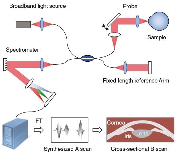
Figure 17. Spectral domain optical coherence tomography (SD-OCT) system with lateral probe beam displacement for cross-sectional B scan imaging. A computer converts the spectrometer data to a synthesized A scan by means of a Fourier Transform. (FT)
Some of the more recent work in OCT has involved full-field imaging (FF-OCT) using 2D camera arrays instead of raster scanning with a point sensor [65]. Many of the optical configurations for such systems, mainly those using TD data acquisition, are almost the same as for CSI microscopy [65]. A key difference being the way in which the data are attained, analyzed, and presented: CSI involves a continuous axial scan during a complete camera frame data acquisition with 0.07 μm displacement between frames, whereas in some implementations, FF-OCT samples the interference fringe contrast at 1 μm intervals using a phase-shifting technique [65]. CSI software signifies surfaces or interfaces between film layers exhibited as surface height z values arranged on an object-space x, y grid, with a height uncertainty on the order of 1 nm, while OCT images display signal strength as a function of depth within the sample volume, frequently with a logarithmic response scale to bring out weak signals, and an anticipated depth resolution on the order of 1 μm. The difference in data analysis and display reflects a difference in application importance, with FF-OCT most closely aligned with life science applications for which surfaces are not as properly defined as with CSI.
The attraction of OCT for life science applications is that it images the internal microstructure in biological tissues by measuring echoes of backscattered light, in a manner resembling ultrasound but at much higher lateral and depth resolutions. Depth resolution for OCT is 1–15 μm, based on the source bandwidth, compared to the 0.1–1 mm resolution of clinical ultrasound [66]; although a limitation when compared to ultrasound is the restricted imaging depth of 2–3 mm within tissue. After wide-ranging trials [66], commercial instruments for ophthalmic diagnostics were launched in 1996. These systems have an important role to play in ophthalmology by identifying early stages of disease prior to physical symptoms and permanent vision loss occurs. OCT can be combined with endoscopes, laparoscopes, catheters, needles, or tethered capsule endomicroscopy, enabling imaging of the internal body [67].
Medical OCT has had the ultimate impact in ophthalmology, where it has become a standard tool for testing the retina, with more than 20 million procedures performed annually at the time when this article was done. Dimensional metrology applications include measuring the thickness of the cornea. Quickly growing applications are for gastrointestinal and cardiovascular diagnostics. Outside the life sciences, OCT imaging can be applied to quality control of multilayered transparent films to art preservation.
Super Resolution Imaging
Although it is connected more with imaging than optical dimensional metrology, it is hard to ignore in this chapter the advances in optical resolution of sub-wavelength features in life science microscopy. Optical imaging and metrology instruments traditionally have been restricted by conventional diffraction limits, quantified by the Sparrow or Rayleigh criteria to nearly half a wavelength under the ideal conditions. However, a number of new technologies have been developed lately that sidestep this limit. These new super-resolution technologies are either based on custom-made illumination, nonlinear fluorophore responses, or the precise localization of single molecules. On the whole, these new methods have created unparalleled new possibilities to examine the structure and function of cells.
Traditional full-field approaches of refining lateral resolution include edge enhancement and modeling on the software side; as well as UV wavelength, confocal, and synthetic illumination on the hardware side (traditional limits). However, none of these methods approach the amazing advances afforded by new techniques that exploit the special properties of fluorescence imaging, which is typical with biological samples (see the section titled “Fluorescence Microscopy,” in Microscopy in The Optics Encyclopedia).
Super-resolution approaches include ground state depletion (GED) and stimulated emission depletion (STED) microscopy, which exploit the nonlinear response of fluorophores; and stochastic optical reconstruction microscopy (STORM) and photo activated localization microscopy (PALM), which identify individual fluorophores that discharge light at separate times to slowly build up an image without the separate emissions overlapping at any one moment in time (refer Figure 18). These methods have been widely reviewed elsewhere [68–70] and are outside the scope of this article, but it is useful to note that these approaches are nowadays regularly resolving features separated by as little as a few tens of nanometers. Many of these techniques also have the ability to resolve depth to a much greater resolving power than conventional confocal microscopy.
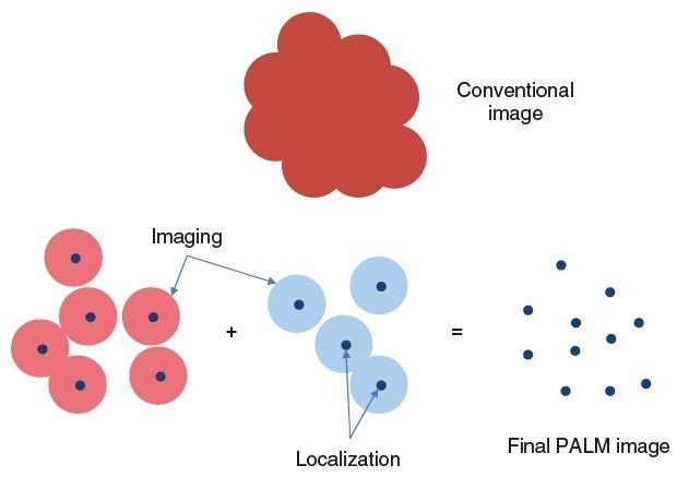
Figure 18. Conventional imaging relies on the detection of irradiance from multiple sources of light from an object at the same time. The overlapping point spread functions lead to blurring (top). However, if the object points emit at different times through fluorescence, they are distinguishable and can be precisely localized at less than the diffraction limit. The final image is reconstructed from a sequence of such time-varying fluorescence images.
The main limitation of the maximum performance super-resolution techniques is the need for fluorescence, which for cellular imaging is not essentially a problem, given the widespread use of fluorescent markers. A more universal full-field super-resolution metrology capability, for instance, for semiconductor lithography or for high-resolution, label-free cellular imaging, remains a crucial area of development for the next generation of optical microscopes.
Conclusion
In these chosen examples of advances in optical metrology, the two trends have been identified in the introduction: improvement in enabling technologies and the growing demand for high precision.
In the case of fiber-based displacement sensors and encoders, the huge advance has been in the demand for precision, mainly driven by the photolithography industry. For encoders, the technology became a vital solution to the contribution of air turbulence to stage positioning uncertainty, which was formerly, but is no longer, tolerable, given the demands of modern semiconductor manufacturing.
The driver for form metrology in tough environments has been the demand for precision in production environments where formerly interferometry was considered both inappropriate and mostly needless. This, in turn, has resulted in solutions enabled by new subsystems, such as pixel-based polarization-sensing cameras, and high-speed computing solutions to the traditional carrier fringe technique.
Deflectometry provides an effective solution for free-form optics and other surfaces that are tough for interferometry. Here, an important advance has been in computing power to facilitate very complex and effective calibration of the system.
In microscopic areal surface topography measurement, focus sensing, structured light, and confocal systems have found new applications in industrial metrology, partly thanks to new cameras, spatial light modulators, and light sources. This consecutively has motivated manufacturers of interference microscopes to develop the sensitivity, ease of use, slope acceptance, and field of view.
OCT has made exceptional advances, owing to new lasers, configurations, and detectors, enabling cross-sectional and 3D volumetric imaging in certain cases at rates a thousand times faster compared to a decade ago.
In conclusion, advanced lasers, new fluorophores, and inventive techniques for forming images with a resolving power outside the conventional diffraction limit provide an effective response to the persistent need for better cellular imaging.
Glossary
Confocal Microscopy: A focus-based imaging and metrology technique that employs physical or virtual apertures to more precisely define the position of best focus, while improving image contrast and lateral resolution.
Deflectometry: A technique for form and roughness metrology that measures dimensional surface details by the way in which the object surface geometrically deflects light paths
Focus Sensing 3D Microscopy: Technique for areal surface topography measurement that relies on the variation in image contrast during a focus scan.
Heterodyne Encoder: Component of a stage-positioning system that employs heterodyne interference phase detection of diffracted light from a grating to measure in-plane motions of the grating.
Optical Coherence Tomography (OCT): Method for cross-sectional or 3D volumetric imaging using scattered light and optical coherence. Usually associated with turbid media and the life sciences, but increasingly of general use.
PALM and STORM: Photo-activated localizationmicroscopy (PALM) and stochastic optical reconstruction microscopy (STORM): widefield super-resolution techniques that build up images by detection and localization of individual fluorophores that emit light at different moments in time.
Structured Illumination Microscopy (SIM): or SIM achieves optical sectioning in a conventional wide-field microscope by projecting a grid pattern onto the object.
Super Resolution: Most generally, any technique that provides imaging capability with a resolving power superior to the diffraction limit.
References
- Badami, V., de Groot, P. (2013), in K. G. Harding (Ed.), Handbook of Optical Dimensional Metrology. Boca Raton: Taylor & Francis, Chap. 4, pp. 157–238.
- de Groot, P. (2001), Opt. Eng. 40, 28–32.
- Abbas, G. L., Babbitt, W. R., de la Chapelle, M., Fleshner, M. L., McClure, J. D., Vertatschitsch, E. J. (1990), Proc. SPIE 1219, 468–479.
- Liu, T. Y., Cory, J., Jackson, D. A. (1993), Appl. Opt. 32, 1100.
- Deck, L. L. (2009), SPIE 7405, 74050E-1–74050E-9.
- de Groot, P. J., Badami, V. G. (2014), in W. Osten (Ed.), Proc. Fringe 2013. Berlin Heidelberg: Springer, Chap. 143, pp. 785–790.
- Badami, V. G., Fletcher, C. D. (2009), 47, 112–115.
- Deck, L. L., de Groot, P. J., Schroeder, M. (2012), US Patent 8,300,233.
- William, R., Trutna, J., Owen, G., Ray, A.B., Prince, J., Johnstone, E. S., Zhu, M., Cutler, L. S. (2008), US Patent 7,440,113.
- Akiyama, K., Iwaoka, H. (1986), US Patent 4,629,886.
- Kao, C.-F., Lu, S.-H., Shen, H.-M., Fan, K.-C. (2008), Jpn. J. Appl. Phys. 47, 1833–1837.
- de Groot, P., Liesener, J. (2013), US Patent 2013/0114061.
- Sykora, D. M., de Groot, P. (2010), Optical Society of America OMA1.
- Smythe, R. (1984), Opt. Eng. 23, 361–364.
- Hettwer, A., Kranz, J., Schwider, J. (2000), Opt. Eng. 39, 960–966.
- Tobiason, J. D., Atherton, K. W. (2005), US Patent 6,847,457.
- Millerd, J. E., Brock, N. J., Hayes, J. B., North-Morris, M. B., Novak, M., Wyant, J. C. (2004), Proc. SPIE 5531, 304–314.
- Kimbrough, B., Millerd, J., Wyant, J., Hayes, J. (2006), Proc. SPIE 6292, 62920F.
- Szwaykowski, P., Bushroe, F. N., Castonguay, R. J. (2011), US Patent 8,004,687.
- Creath, K., Goldstein, G. (2012), Proc. SPIE 8227, 82270M–82270M-10.
- Zhao, C., Kang, D., Burge, J. H. (2005), Appl. Opt. 44, 7548–7553.
- Takeda, M., Ina, H., Kobayashi, S. (1982), J. Opt. Soc. Am. 72, 156.
- Ichioka, Y., Inuiya, M. (1972), Appl. Opt. 11, 1507.
- Sykora, D. M., de Groot, P. (2011), Proc. SPIE 8126, 812610–812610-10.
- Sykora, D. M., Kuechel, M. (2013), US Patent Application 20130063730.
- de Groot, P. (2012), Proc. EUSPEN 1, 31–34.
- Coulombe, A., Brossard, M. C., Nikitine, A. (2006), US Patent 7,023,559.
- Malacara-Doblado, D., Ghozeil, I. (2006), Optical Shop Testing. Hoboken: John Wiley & Sons, Inc., pp. 361–397.
- Su, P., Parks, R. E., Wang, L., Angel, R.P., Burge, J. H. (2010), Appl. Opt. 49, 4404–4412.
- Juptner, W., Bothe, T. (2009), Proc. SPIE 7405, 740502–740502-8.
- Faber, C., Olesch, E., Krobot, R., Häusler, G. (2012), Proc. SPIE 8493, 84930R–84930R-15.
- Hausler, G., Knauer, M. C., Faber, C., Richter, C., Peterhänsel, S., Kranitzky, C., Veit, K. (2009), in W. Osten, M.Kujawinska (Eds.), FRINGE 2009: The 6th International Workshop on Advanced Optical Metrology. Heidelberg: Springer, pp. 416–421.
- Knauer, M. C., Kaminski, J., Hausler, G. (2004), Proc. SPIE 5457, 366–376.
- Faber, C. (2012), New Methods and Advances in Deflectometry. Ph.D. Thesis, Friedrich-Alexander-University of Erlangen-Nuremberg.
- Su, P., Wang, Y., Burge, J. H., Kaznatcheev, K., Idir, M. (2012), Express 20, 12393–12406.
- Helmli, F. (2011), in R. Leach (Ed.), Optical Measurement of Surface Topography. Berlin Heidelberg: Springer, Chap. 7, pp. 131–166.
- Geng, J. (2011), Adv. Opt. Photonics 3, 128.
- Engelhardt, K., Hausler, G. (1988), Appl. Opt. 27, 4684–4689.
- Colonna de Lega, X. M. (2014), US Patent 8,649,024.
- Neil, M. A. A., Juskaitis, R., Wilson, T. (1997), Opt. Lett. 22, 1905–1907.
- Wilson, T., Sheppard, C. (1984), Theory and Practice of Scanning Optical Microscopy. London: Academic Press.
- Nipkow, P. (1885), German Patent 30105.
- Xiao, G. Q., Corle, T. R., Kino, G. S. (1988), Appl. Phys. Lett. 53, 716–718.
- Ishihara, M., Sasaki, H. (1999), Opt. Eng. 38, 1035–1040.
- Artigas, R. (2011), in R. Leach (Ed.), Optical Measurement of Surface Topography. Berlin Heidelberg: Springer, Chap. 11, pp. 237–286.
- Bradl, J., Rinke, B., Esa, A., Edelmann, P., Krieger, H., Schneider, B., Hausmann, M., Cremer, C. G. (1996), Proc. SPIE 2926, 201–206.
- Molesini, G., Pedrini, G., Poggi, P., Quercioli, F. (1984), Opt. Commun. 49, 229–233.
- Tiziani, H. J., Uhde, H. M. (1994), Appl. Opt. 33, 1838.
- Leach, R. K. (Ed.), (2013), Characterisation of Areal Surface Texture. Heidelberg: Springer.
- Sachs, R., Stanzel, F. (2014), in W. Osten (Ed.), Fringe 2013. Berlin Heidelberg: Springer, Chap. 96, pp. 535–538.
- Deck, L. L. (2007), SPIE Technical Digest TD04, Paper TD040M.
- de Groot, P. (2011), in R. Leach (Ed.), Optical Measurement of Surface Topography. Berlin: Springer Verlag, Chap. 9, pp. 187–208.
- Fay, M. F., Colonna de Lega, X., de Groot, P. (2014), Classical Optics 2014, OSA Technical Digest. Paper OW1B.3.
- Dresel, T., Häusler, G., Venzke, H. (1992), Appl. Opt. 31, 919–925.
- de Groot, P. J., Colonna de Lega, X., Grigg, D. A. (2002), Proc. SPIE 4778, 127–130.
- de Groot, P. J., Deck, L. L., Biegen, J. F., Koliopoulos, C. (2011), US Patent 8,045,175.
- de Groot, P. J., Biegen, J. F. (2015), Proc. SPIE 9525, 95250N–95250N-7.
- de Groot, P. J., Colonna de Lega, X. (2004), Proc. SPIE 5457, 26–34.
- Colonna de Lega, X. (2012), in W. Osten, N. Reingand (Eds.), Optical Imaging andMetrology. Weinheim: Wiley-VCH Verlag GmbH & Co. KGaA, Chap. 13, pp. 283–304.
- de Groot, P., Colonna de Lega, X., Liesener, J. (2009), in W. Osten, M. Kujawinska (Eds.), Fringe 2009. Berlin: Springer Verlag, pp. 236–243.
- Fercher, A. F., Mengedoht, K., Werner, W. (1988), Opt. Lett. 13, 186–188.
- Swanson, E. A., Huang, D., Lin, C. P., Puliafito, C. A., Hee, M. R. (1992), Opt. Lett. 17, 151–153.
- Huang, D., Swanson, E. A., Lin, C. P., Schuman, J. S., Stinson, W. G., Chang, W., Hee, M. R., Flotte, T., Gregory, K., Puliafito, C. A., Fujimoto, J. G. (1991), Science 254, 1178–1181.
- Choma, M. A., Sarunic, M. V., Yang, C., Izatt, J. A. (2003), Express 11, 2183–2189.
- Dubois, A., Boccara, A. C. (2008), in W. Drexler, J. Fujimoto (Eds.), Optical Coherence Tomography. Berlin Heidelberg: Springer, Chap. 19, pp. 565–591.
- Fujimoto, J., Drexler, W. (2008), in W. Drexler, J. Fujimoto (Eds.), Optical Coherence Tomography. Berlin Heidelberg: Springer, Chap. 1, pp. 1–45.
- Gora, M. J., Sauk, J. S., Carruth, R.W., Gallagher, K. A., Suter, M. J., Nishioka, N. S., Kava, L. E., Rosenberg, M., Bouma, B. E. (2013), Nat. Med. 19, 238–240.
- Toomre, D., Bewersdorf, J. (2010), Ann. Rev. Cell Develop. Biol. 26, 285–314.
- Huang, B., Bates, M., Zhuang, X. (2009), Ann. Rev. Biochem. 78, 993–1016.
- Schermelleh, L., Heintzmann, R., Leonhardt, H. (2010), J. Cell Biol. 190, 165–175.

This information has been sourced, reviewed and adapted from materials provided by Zygo Corporation.
For more information on this source, please visit Zygo Corporation.