The outstanding properties of 2D materials for critical applications in semiconductors, battery technology, photovoltaics, and numerous other areas render them a key emerging field of research. Numerous nanoscale and microscopy techniques have been employed to characterize 2D materials to achieve clearer understandings of the nature of their properties. NanoIR techniques expand this characterization with essential nanoscale chemical and optical property mapping.
The nanoIR3-s system provides two complementary nanoscale IR techniques, AFM-IR photothermal-based nanoscale IR imaging and spectroscopy (including Tapping AFM-IR) and scattering-scanning near-field optical microscopy (s-SNOM). Such techniques provide a remarkable comprehension of the nanoscale chemical and complex optical properties of 2D materials.
Complementary atomic force microscopy (AFM) techniques like mechanical and thermal property mapping also present information on the mechanical, thermal, and electrical properties of such materials. These techniques permit chemical and optical property mapping with 10 nm spatial resolution, which is far less than the diffraction limit of conventional IR spectroscopy.
In this article, the use of the nanoIR3-s system for characterizing a variety of 2D structures and materials, including graphene, nanoantennae, semiconductors, and more, is detailed.
Complementary Nanoscale IR Techniques
The nanoIR3-s has the capacity to acquire nanoscale images and IR spectra employing two distinct near-field spectroscopy techniques: s-SNOM and photothermal AFM-IR. These complementary techniques allow nanoscale chemical assessment, in addition to mechanical, electrical, thermal, and optical mapping with spatial resolution as low as a few nanometers for hard and soft matter applications.
Nanoscale IR spectroscopy combines the precise chemical recognition of infrared spectroscopy with the nanoscale capacities of AFM to allow chemical recognition of sample components at a chemical spatial resolution as low as 10 nm with monolayer sensitivity, breaking the diffraction limit by more than 100x.
AFM-IR absorption spectra are precise measurements of sample absorption and do not rely on other complex optical elements of the sample and the tip. As such, the spectra compare exceptionally well to that of conventional bulk transmission IR.
Imaging of Plasmons and Phonons
Because of their elevated spatial confinement, surface plasmon polaritons (SPPs) and surface phonon polaritons (SPhPs) in 2D materials can produce new opportunities for enhanced light-matter contact, subwavelength metamaterial, super lenses, and additional innovative photonic devices.
A flexible optical imaging and spectroscopy tool with nanometer spatial resolution is necessary for the in-situ characterization of such polaritonic excitations throughout several applications. s-SNOM provides an excellent way to selectively motivate and locally identify vibrational and electronic resonances in real space via a non-invasive near-field light-matter collaboration.
This technique is shown by imaging the SPhPs of hexagonal boron nitride (hBN), as shown in Figure 1. Corresponding information for a comprehensive characterization of the polaritonic resonances is presented by amplitude and phase near-field optical images. The observation of over 90° phase shift of SPhPs on hBN indicates solid light-matter coupling.
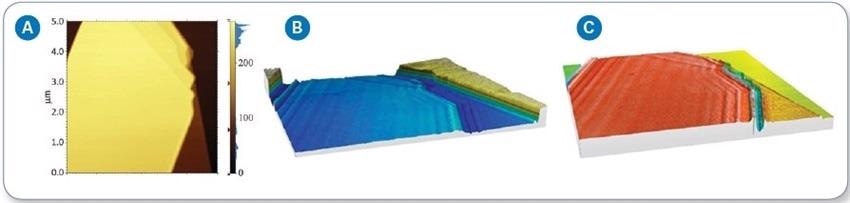
Figure 1. (a) AFM height image shows homogeneous hBN surface with different layers on a Si substrate; (b) s-SNOM amplitude shows strong interference fringes due to propagating SPhP along the surface on hBN; (c) s-SNOM phase shows a different phase signal with layer thickness. Image Credit: Bruker Nano Surfaces
The SPPs of graphene can additionally be studied employing the nanoIR3-s analogous to the visualization of the SPhPs in hBN. The standing wave of an SPP on a graphene wedge can be seen in Figure 2. Typically, only the end radius of the AFM probe restricts the spatial resolution of s-SNOM, thus permitting the s-SNOM method to record the cross sections of SPP as low as nearly 8 nm.
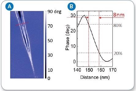
Figure 2. (a) s-SNOM phase image of surface plasmon polariton on graphene; (b) cross section of SPP standing wave phase. Image Credit: Bruker Nano Surfaces
Nanocontamination of Graphene
The distinctive electrical and mechanical properties of graphene depend on the maintenance of the total conjugated composition of the sheet. The nanoIR3-s can assess the value of exfoliated graphene achieved by various methods, seen in Figure 3. Contamination that is not easily identifiable in the AFM height image is noticeable in the s-SNOM reflection image. Discrepancies in the s-SNOM reflection image alter according to the number of existing graphene layers, displaying nano contamination on the sample.
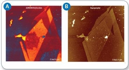
Figure 3. (a) s-SNOM reflection image, showing nanocontamination (dirt), and (b) AFM height image of exfoliated graphene. Image Credit: Bruker Nano Surfaces
Characterizing Nanoantenna Resonance
Nanoantennae possess a broad variety of applications, differing from sensing to energy conversion. For the production of precise and dependable devices, the capacity of quantifying and tuning the resonance formations of these antennas is of vital significance. Arrays of nanoantennae are common as they permit many individual antennas to be packed inside a small area. An AFM topography image of an antenna array including coupled antennas and single bar antennas can be seen in Figure 4a.
The contact point to the antennas is a crucial component in accomplishing ideal energy transfer efficiency throughout the production of antenna arrays. s-SNOM imaging allows simple detection of the antenna resonance hot spots and the ideal contact point. The s-SNOM amplitude and phase image of a single bar antenna included within the array can be seen in Figure 4b. The dipole antenna resonance may be seen with 11 µm excitation. A phase shift of ~180° can be seen at dipole resonance.
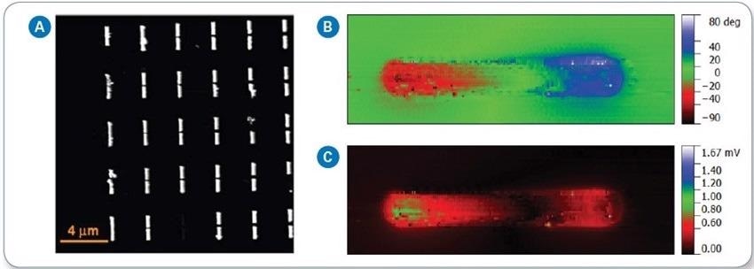
Figure 4. (a) AFM height image of assembled antenna array, (b) s-SNOM phase, and (c) s-SNOM amplitude images of antenna dipole. Image Credit: Bruker Nano Surfaces
In addition to the capability to accumulate high-resolution images of optical phenomenon, the nanoIR3-s provides the capacity to spectrally probe nanoscale surface characteristics.
Figure 5 displays the AFM-IR spectra accumulated on single rod and coupled antenna, on which the antenna resonance can be noticeably resolved at 910 cm-1, in agreement with theoretical projections.
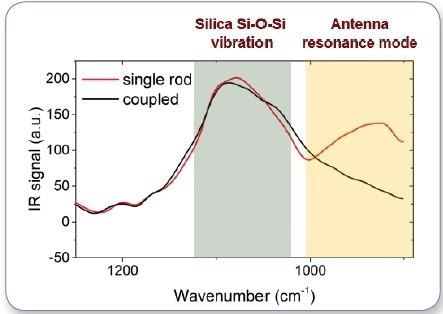
Figure 5. AFM-IR spectrum collected on single rod and coupled antenna; the peak at 910 cm-1 corresponds to the antenna resonance of the single rod antenna, while the peak at 1100 cm-1 shows the Si-O mode shared by both antennas. Image Credit: Bruker Nano Surfaces
Effects of Polarized Light on Metasurface Chirality
This is the first time the combination of complementary nanoscale imaging techniques, s-SNOM and AFM-IR, have been employed to examine the role of chirality in the beginnings of circular dichroism in 2D nanoscale materials.
Chiral molecules are a particular type of molecule that possess a non-superimposable mirror image. The mirror images of chiral molecules are known typically as left-handed and right-handed, and due to the vector nature of light, it can also occur with two types of handedness, left and right circularly polarized.
Completely two-dimensional (2D) metamaterials, also known as metasurfaces, comprised of planar-chiral plasmonic metamolecules with a thickness of a small number of nanometers, have demonstrated chiral dichroism in transmission (CDT). Theoretical calculations indicate that this unanticipated impact is reliant on finite non-radiative (ohmic) losses of the metasurface. To date, this surprising theoretical expectation has not been experimentally verified because of the complexity in recording the non-radiative loss on the nanoscale.
s-SNOM is employed to map the optical energy allocation when the structures are exposed to RCP and LCP IR radiation; in contrast, AFM-IR was then employed to identify the fundamentally distinct ohmic heating shown under RCP and LCP radiation.1
It has been irrefutably proven for the first time that the circular dichroism seen in 2D metasurfaces can be credited to handedness-dependent ohmic heating, displayed in Figure 6.
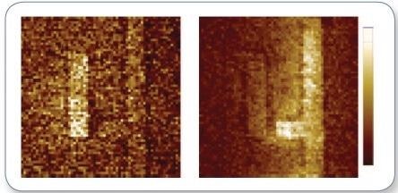
Figure 6. Experimentally measured AFM cantilever deflection amplitudes. The cantilever deflection is directly proportional to temperature increase in the sample during the laser pulse; this confirms that the magnitude and spatial distribution the Ohmic heating of a chiral 2D metasurface markedly depends on the handedness of light1. Image Credit: Bruker Nano Surfaces
Analysis of Carbon Nanotubes with nanoIR
The AFM-IR method works by identifying the thermal expansion of a material caused by the absorption of infrared illumination. A material’s thermal expansion is dependent on many factors, like the thickness of the material and the coefficient of thermal expansion. 1D and 2D materials, like single-walled carbon nanotubes (CNT) and single-layer graphene, have a low coefficient of thermal expansion in addition to a thickness of around 1–2 nm. Characterization with AFM-IR is made problematic because of the nature of these 1D and 2D samples.
A two orders of magnitude increase in AFM-IR signal strength is seen by placing a thin layer of polymeric material beneath the graphene and CNT samples.2,3 Because the incident IR radiation is absorbed by the thin sample absorbs, the produced heat is transferred to the thin polymer that has a significantly larger coefficient of thermal expansion, causing it to expand.
Figure 7 displays the finite element analysis model employed to replicate the impacts that polymer thickness has on the temperature changes and thermal expansion.
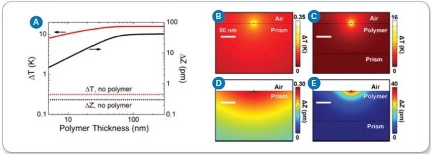
Figure 7. (a) Temperature rise (ΔT) and expansion (ΔZ) as a function of polymer thickness beneath the sample; Temperature rise (b) with no polymer and (c) with polymer beneath the sample; Vertical thermomechanical expansion (d) with no polymer and (e) with polymer beneath the sample. Image Credit: Bruker Nano Surfaces
The model was validated by inspecting a series of CNTs positioned above a 150 nm thick polystyrene layer on a ZnSe prism. Prior to CNT deposition, an area of the polymer substrate was taken away to guarantee there was an area of CNT that did not have polymer underneath. Figure 8 shows that the IR chemical image achieved at 4000 cm-1 displays a clear signal from the CNT in the region which has polystyrene below, while no signal is evident where the polymer substrate has been taken away. It has been indicated that the altering AFM-IR signal from various CNTs is due to the difference between metallic and semiconducting tubes.
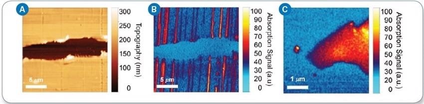
Figure 8. (a) AFM topography imaging of CNTs deposited on polystyrene substrate; (b) IR chemical mapping image at 4000 cm-1 showing absorption by CNTs; (c) IR chemical mapping image of monolayer graphene captured at 4000 cm-1. Image Credit: Bruker Nano Surfaces
The AFM-IR imaging of graphene above a 106 nm thick layer of PMMA is shown in Figure 8c. This image shows the extension of this method to monolayer 2D materials.
Because of the amplification of the AFM-IR signal by a thin layer of polymer, the signal strength is strengthened by two orders of magnitude. This new method allows the AFM-IR characterization of 1 nm thick 1D and 2D materials, which was not feasible before. In the future, this substantial signal increase may be used in a variety of applications, such as ultrathin biologicals and a number of 1D and 2D materials.
Investigating Exothermic Peaks of Polyethylene Using nanoTA and LCR
An extremely popular and widely used polymer is polyethylene (PE), with functions in numerous industries, such as 2D materials applications. Inorganic fillers like graphite and metallic particles have been included to alter the thermal, electrical and mechanical properties of PE.
Hexagonal boron nitride (hBN) has shown capacity as a filler due to its great mechanical strength, insulating properties, and thermal conductivity. Researchers at Sichuan University described this impact of hBN particles on the melting performance of polyethylene employing Lorentz Contact Resonance (LCR) and nano-thermal analysis (nanoTA).3
Figures 9a and b show that LCR imaging can vividly display areas of great hBN concentration on the surface. After, nanoTA was employed to measure the softening temperature of various areas in the material; displayed in Figure 9, an increase in the transition temperature of 4–8 °C was seen for regions of the PE sample near hBN aggregates when contrasted with regions not possessing hBN.
Employing the bulk transition temperature throughout the basic deviation of the nanoTA values, the precision of this method was validated in contrast with traditional DSC analysis.
These outcomes, combined with DSC analysis, show that the meso-phase of the PE develops close to h-BN particles throughout crystallization, which creates a weak exothermic peak that was previously unsolved.
Displayed in Figure 9 is nanoTA measurement also performed directly on the hBN particles, for which no thermal transition was calculated at temperatures up to 400 °C.
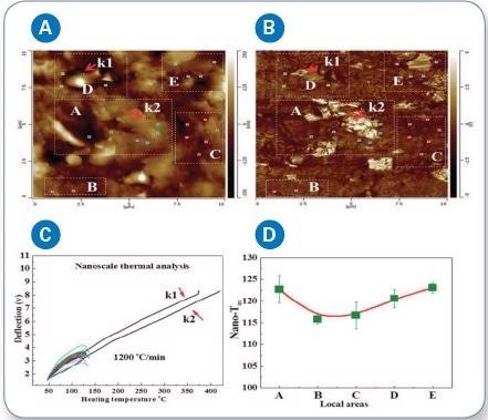
Figure 9. (a) LCR-AFM height image; (b) AFM mechanical image (using LCR) of the PE/BN composites, showing boron nitride clusters in the areas A, D, and E; (c) Local thermal analysis data of the assigned positions were obtained by nano-TA, comparing the melting temperatures of PE and BN; (d) DSC from the PE/BN composites (heating rate of 2 °C min-1). Image Credit: Bruker Nano Surfaces
Analyzing Thermal Conductivity of Graphene Sheets with SThM
The latest research has concentrated on graphene due to its high thermal conductivity and potential in optoelectronics. Scanning Thermal Microscopy (SThM) characterizes thermal conductivity of 2D materials as it produces high sensitivity in resistance recognition between the probe and the sample. These elevated spatial resolutions remove ambiguity in the detection of the source of a sample’s electrical capabilities, which renders SThM a trustworthy method for monitoring sample temperature and, additionally, thermal conductivity in a qualitative manner.
Researchers at Durham University and Lancaster University used SThM to examine the thermal conductivity of single and multilayer graphene sheets.4 Graphene was deposited on Si/SiO2 substrate with pre-patterned trenches, with both graphene suspended over the trench and reinforced by the substrate imaged. It was found that a rise in the number of reinforced graphene layers caused an apparent reduction in thermal resistance.
A key observation was that the thermal conductance of both bilayer and multilayer graphene suspended above the trench was greater than that of the supported layer, compared to expectations that conduction from the graphene to the substrate would produce more heat dissipation.
Because the mean free path of thermal phonons in graphene is considerably larger when contrasted to the height of the trench, it is hypothesized that ballistic acoustic phonons from the SThM tip are the main cause of heat transfer, with 90% approaching the trench in the ballistic regime. A graphene bulge that was still suspended above the trench displayed comparable properties, eliminating experimental differences such as SThM contact region as the trigger of such behavior.
These measurements determined that three-layer graphene had almost 68% of the thermal conductance than the single layer. Lastly, thermal mapping of border areas between supported graphene layers shows that the thermal transition area has a width of 50–100 nm, confirming hypothetical estimations for the mean free path.
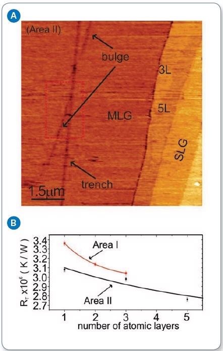
Figure 10. (a) SThM image of supported graphene, showing varied thicknesses throughout the sample; (b) measured contact thermal resistance as a function of the number of graphene layers, showing reduction in thermal resistance as the number of layers increases. Image Credit: Bruker Nano Surfaces
Conclusion
The nanoIR3-s provides excellent characterization of 2D material properties with complimentary photothermal-based Tapping AFM-IR and near-field s-SNOM techniques. AFM-based nanoscale property mapping provides correlative microscopy capacity for electrical, thermal, and mechanical property mapping.
References
- Khanikaev AB, Arju N, Fan Z, Purtseladze D, Lu F, Lee J, Sarriugarte P, Schnell M, Hillenbrand R, Belkin MA, Shvets G. Experimental demonstration of the microscopic origin of circular dichroism in two-dimensional metamaterials. Nature Communications. 2017.
- Rosenberger MR, Wang MC, Xie X, Rogers JA, N S, K WP. Measuring individual carbon nanotubes and single graphene sheets using atomic force microscope infrared spectroscopy. Nanotechnology. 2017.
- Zhang X, Wu H, Guo S, Wang Y. 2015. Understanding in crystallization of polyethylene: the role of boron nitride (BN) particles. Royal Social of Chemistry Advances. 2015(121):99585-100407.
- Pumarol ME, Rosamond MC, Tovee P, Petty MC, Zeze DA, Falko V, Kolosov OV. Direct Nanoscale Imaging of Ballistic and Diffusive Thermal Transport in Graphene Nanostructures. Nano Letters. 2012(12)2906-2911.

This information has been sourced, reviewed and adapted from materials provided by Bruker Nano Surfaces.
For more information on this source, please visit Bruker Nano Surfaces.