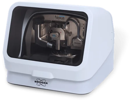
Dimension Nexus™ offers an ideal combination of data quality, experimental flexibility, and ease of use in a compact system. It features Bruker's milestone innovations, including the NanoScope® 6 controller, PeakForce Tapping® technology, and ScanAsyst® Plus self-optimizing imaging software, delivering more functionality than other systems in its class.
Suitable for both routine and custom experiments and easily upgradable in the field, Dimension Nexus is a strong entry-level option and a valuable addition to any established AFM lab.
Dimension Nexus: A New High-Performance Standard for Cost-Effective AFMs
Video Credit: Bruker Nano Surfaces and Metrology
- Best-in-Class Performance: Allows for imaging at atomic and molecular resolutions.
- Ultimate Versatility and Value: Provides a wide range of AFM modes.
- Programmable Motorized Stage: Improves productivity for publication-ready results.
Features
Provides Core Performance and Value in Every Scan
Nexus routinely produces highly accurate, reproducible, publication-ready results for a variety of sample types in both research and industrial settings.
Ensuring High Performance
At the core of this system’s best-in-class performance is its integrated suite of advanced hardware, software, and accessories, including:
- A full range of PeakForce Tapping modes, enabling high-resolution imaging and quantitative mapping of mechanical, electrical, and chemical properties across the broadest variety of samples.
- The latest-generation NanoScope 6 controller offers ultra-low noise, high-speed performance, and exceptional versatility for unmatched capabilities and ease of use.
- An XYZ closed-loop scanner, drift-compensated bridge design, and integrated granite base, delivering high-performance results for small samples on an open-access, large-sample AFM.
- The most extensive selection of dedicated AFM probes, each optimized for specific modes and sample types.
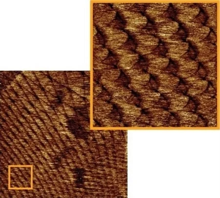
High-resolution topography images of a van der Waals heterostructure showing a moiré superlattice. Images collected in torsional resonance dynamic force microscopy (TR-DFM) with a FESPA probe. Scan sizes 1x1 µm and 200x200 nm (orange box). Image Credit: Bruker Nano Surfaces and Metrology
Guaranteeing Stability
Dimension Nexus has little drift when imaging for extended periods of time, and it does not show any scanner artifacts or tip degradation over lengthy scan lengths.
![[Top] Beginning and ending of a 360-trench array in PeakForce Tapping using a SAA-HPI probe, with a total scan size of 90×2 µm (16384×16 pixels). Over the entire range, critical dimension analysis revealed no signs of tip degradation or scanner artifacts. [Bottom] Pitch measurements from trench to trench in all 360 trenches, displaying almost negligible variation throughout the scan range.](https://www.azonano.com/images/equipments/EquipmentImage_2289_17470267274146899.png)
[Top] Beginning and ending of a 360-trench array in PeakForce Tapping using a SAA-HPI probe, with a total scan size of 90×2 µm (16384×16 pixels). Over the entire range, critical dimension analysis revealed no signs of tip degradation or scanner artifacts. [Bottom] Pitch measurements from trench to trench in all 360 trenches, displaying almost negligible variation throughout the scan range. Image Credit: Bruker Nano Surfaces and Metrology
Delivers Outstanding Value and Ease of Use
For researchers who are just starting out in their labs or who intend to grow their AFM research in the future, Nexus offers clear benefits:
- The base configuration includes a programmable stage for high-throughput, multi-site measurements, which quickly yields high-quality data for common applications
- Operators of all experience levels can get consistent results, thanks to user-friendly features such as fast sample/probe setup, ScanAsyst self-optimizing imaging, and powerful data analysis software
- Extensive upgrade options — including distinct working modes, dependable environmental control, and sophisticated software integrations — ensure that the system can expand with the study
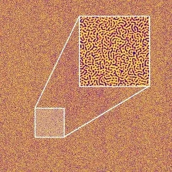
Phase image of styrene butadiene block copolymer (SBC), collected in TappingMode with an RTESPA probe. Full scan size is 5x5 µm, 2560x2560 px. Inset is a digital zoom showcasing the data density and level of detail retained. Image Credit: Bruker Nano Surfaces and Metrology
Offers Future Versatility and Customization
In addition to its upgradability, Dimension Nexus offers open-access design to support experiment customization. The system provides physical access to the probe-sample junction, allowing for the integration of electrical connections and other custom accessories.
The NanoScope 6 controller further supports this flexibility with an open hardware and software platform, featuring front-panel BNC connectors, scripting options, and straightforward data import into Python for custom analysis.
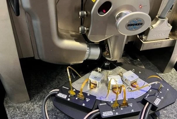
Microprobers integrated with Dimension Nexus for electrical characterization of nanodevices. Image Credit: Bruker Nano Surfaces and Metrology
Applications
Enables Full Range of Applications
With a 150 mm open-access programmable stage, full compatibility with over 50 of Bruker’s AFM modes—including PeakForce Tapping, fluid imaging, and environmental control—Dimension Nexus offers cost-effective, high-performance AFM for a wide range of applications and experiments, including:
- Mapping nanomechanical properties of polymers and composite materials.
- Characterizing graphene, moiré superlattices, and other 2D materials at the nanoscale.
- Correlating structural and ferroelectric properties of perovskites in photovoltaic research.
- Conducting in-situ and operando studies of local electrochemical activity in lithium-ion batteries.
- Quantifying nanoscale surface roughness of semiconductor thin films and substrates.
- Manipulating and characterizing the electrical properties of DNA nanowires for nanoelectronic device development.
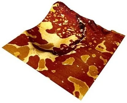
PeakForce quantitative nanomechanics (PeakForce QNM®) can be used to map distribution of components in polymer blends. PS-PMMA-PVC sample courtesy of U. Mons. Scan size 5x5 µm, RTESPA-150 probe. Image Credit: Bruker Nano Surfaces and Metrology
Specifications
Dimension Nexus select specifications. Source: Bruker Nano Surfaces and Metrology
| |
|
| X-Y Scan Range |
90 μm x 90 μm typical, 85 μm minimum |
| Z Range |
10 μm typical in imaging and force curve modes, 9.5 μm minimum |
| Sample Size/Holder |
150 mm vacuum chuck for samples, ≤150 mm diameter, ≤15 mm thick |
| Motorized Positioning (XY Stage) |
150 mm x 150 mm inspectable area; 6 μm repeatability, bidirectional; programmable for multi-site measurements |
| Microscope Optics |
5 MP digital camera; 180 μm to 1465 μm viewing area; digital zoom and motorized focus |
| Certification |
CE |
What Dimension AFM is Right
Bruker offers a broad range of high-quality AFM systems, with the Dimension family showcasing industry-leading imaging and characterization technologies developed through decades of experience and close collaboration with researchers.
At the top of the line, the Dimension Icon sets the benchmark for commercial AFM performance. Now, Dimension Nexus joins the portfolio, delivering outstanding value and capabilities in a more cost-effective system.
NEW Dimension Nexus - best-in-class general purpose AFM. Image Credit: Bruker Nano Surfaces and Metrology
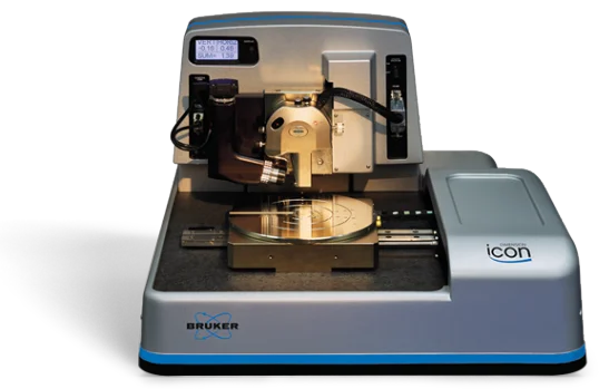
Dimension Icon - gold standard for advanced large-sample AFMs. Image Credit: Bruker Nano Surfaces and Metrology
Key Features and Specs
Source: Bruker Nano Surfaces and Metrology
| |
Dimension Nexus |
Dimension Icon |
| Sample Size (XY) |
150 mm |
300 mm |
| Motorized Stage Range |
150 mm x 150 mm |
150 mm x 180 mm |
| Small & Multi-Sample Compatibility |
Yes |
Yes |
| Sample Flexibility |
Tip Scanner |
Tip Scanner |
| XY-Scan Range |
90 µm x 90 µm |
90 µm x 90 µm |
| Z-Range |
10 µm |
10 µm |
| System Footprint (W x L) |
24" x 32" (plus customer desk/workstation) |
47" x 94" (including integrated workstation) |
| Controller |
NanoScope 6 |
NanoScope 6 |
| Programmable Measurements |
Yes |
Yes |
| Automated Metrology Recipes |
No |
Yes |
| Open-Access Platform |
High degree of flexibility for customization |
Maximum flexibility for customization |
Measurement Capabilities
Source: Bruker Nano Surfaces and Metrology
| |
Dimension Nexus |
Dimension Icon |
| High-Resolution Imaging |
Atomic lattice resolution |
Atomic defect resolution |
| High-Speed Imaging |
Fast Tapping |
FastScan dedicated high-speed AFM; Fast Tapping |
| PeakForce Tapping |
Yes |
Yes |
| ScanAsyst (Self-Optimizing Imaging) |
Yes |
Yes |
| PeakForce Tapping Derivative Modes |
Yes |
Yes |
| Chemical Identification Capability |
No |
IconIR upgradable |
| Hyperspectral Imaging |
DataCube |
DataCube |
| Other Modes & Options |
Wide range to address majority of applications |
Complete range for industry-leading application coverage |
Software
Powered by the NanoScope 6 AFM Controller
With faster performance, lower noise, and expanded AFM mode support, the NanoScope 6 controller unlocks the full capabilities of Bruker’s high-performance Dimension and MultiMode systems. This latest-generation controller delivers exceptional accuracy, precision, and versatility for nanoscale surface measurements across all applications.
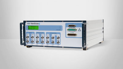
NanoScope 6 AFM controller. Leading-edge AFM controller built on an innovative high-speed, low-noise architecture for delivering unprecedented measurement performance. Image Credit: Bruker Nano Surfaces and Metrology
NanoScope 6 uniquely enables Bruker AFMs to:
- Operate in more imaging modes than competing systems, including advanced and proprietary modes that require complex control and analysis.
- Capture accurate, quantitative data for nanoelectrical and nanomechanical property measurements across diverse sample types.
- Fine-tune scanning parameters to meet even the most demanding research and industrial measurement needs.
- Maximize ease of use with Bruker’s exclusive ScanAsyst® Plus self-optimizing imaging software, powered by advanced intelligent algorithms and patent-pending smart functionality.