Bruker's Dimension IconIR integrates nanoscale infrared (IR) spectroscopy with scanning probe microscopy (SPM) to provide unparalleled performance in spectroscopy, imaging, and property mapping, all on a single platform.
Boasting high-resolution chemical imaging with monolayer sensitivity, the system's large-sample architecture ensures ultimate sample flexibility while preserving all the industry-leading AFM measurement capabilities of the Dimension Icon®.
Dimension IconIR employs Bruker-exclusive PeakForce Tapping® nanoscale property mapping and proprietary nanoIR spectroscopy technology to facilitate correlative microscopy for nanochemical, nanoelectrical, and nanomechanical characterization of materials and active nanoscale systems, even in electrically or chemically reactive environments.

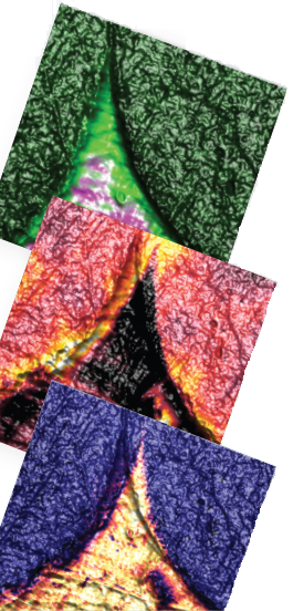
Correlated nanoscale property mapping showing nanoelectrical (PF-KPFM, top), nanothermal (SThM, middle), and nanochemical (AFM-IR, bottom) images of carbon fibers embedded in epoxy resin. Image Credit: Bruker Nano Surfaces and Metrology
Only Dimension IconIR Delivers:
- High-performance nanoIR spectroscopy, <10 nm chemical resolution, monolayer sensitivity, and FT-IR correlation.
- PeakForce Tapping in conjunction with nanomechanical and nanoelectrical modes for correlational chemical imaging.
- Optimal sample flexibility and AFM imaging performance.
- The largest assortment of AFM accessories and modes.
Highest Performance NanoIR Spectroscopy

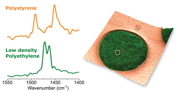
High-quality resonance-enhanced AFM-IR spectra collected at different sites on a PS-LDPE polymer blend, illustrating a high degree of material sensitivity and deeper insight into nanoscale material properties. Image Credit: Bruker Nano Surfaces and Metrology
Bruker is a leader in AFM-IR-based nanoIR spectroscopy thanks to its patented, unique suite of nanoIR modes, providing the highest performance, high-speed, repeatable, and accurate spectra that correlate to FT-IR. The variety of modes on offer allows users to measure a wide range of samples, regardless of whether they are an industrial or academic user.
Dimension IconIR delivers highest performance, and rich, detailed spectra with FT-IR correlation, achieved with single molecular spectroscopy. It enables Resonance Enhanced AFM-IR, the most-published technique in the nanoIR community.
Highest Resolution Chemical Imaging

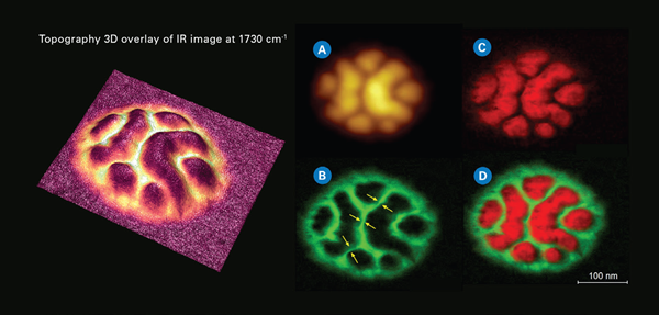
High-resolution chemical imaging of PS-b-PMMA block copolymer in Tapping AFM-IR mode showing sample topography (a); IR images at 1730 (b); and 1492 cm-1 (c) highlighting PMMA and PS, respectively. The yellow arrows in panel (b) indicate chemical resolution <10 nm. The overlay image (d) captures the composition map. Image Credit: Bruker Nano Surfaces and Metrology
The industry-leading AFM performance of the base Dimension Icon platform has enhanced the spatial resolution capabilities of nanoIR technology, making it possible to create the ultimate nanoscale chemical imaging system with sub-10 nm chemical resolution and monolayer sensitivity.
Bruker’s patented Tapping AFM-IR imaging technology has been used for a variety of soft samples, ensuring consistent, reliable, and high-quality publishable data.
IconIR Provides:
- <10 nm chemical spatial resolution for imaging for a wide variety of sample types
- Imaging of thin films and biological structures with monolayer sensitivity
Specifications
Source: Bruker Nano Surfaces and Metrology
| . |
. |
| nanoIR Modes |
Resonance Enhanced AFM-IR; Tapping AFM-IR;
FASTmapping; Contact AFM-IR |
| XY Scan Range |
90 μm x 90 μm typical;
85 μm minimum with Dimension AFM scanner |
| Z Range |
10 μm typical in imaging and force curve modes;
9.5 μm minimum |
| AFM Vertical Noise Floor |
≤50 pm RMS |
| Sample Size |
150 mm diameter vacuum chuck;
<15 mm thick |
| Large XY Motorized Position Stage |
X-Y Travel is 150 mm x 150 mm |
| Microscope Optics |
5 MP digital camera; 180 μm to 1465 μm viewing area;
Digital zoom and motorized focus |
| Acoustic Hood and Isolation Table |
Required to meet performance specifications in environments with up to 75 dBC continuous acoustic noise when used with acoustic hood |
| Purging Hood |
Available for purging environment using CDA |
| Nanomechanical Modes (optional) |
PeakForce QNM® and variants;
AFM-nDMA; FASTForce Volume™; RampScript™ |
| PeakForce Nanoelectrical Modes (optional) |
PeakForce TUNA™; DCUBE-TUNA;
PeakForce KPFM™; PeakForce sMIM; DCUBE-sMIM |
| Nanoelectrical Modes (optional) |
CAFM; SSRM; DarkLift |
| Other Capabilities (optional) |
AutoMET® for AFM; Fast Tapping; Fluid Imaging |