The InSight 300 is a fab-ready automated atomic force microscope (AAFM) built for reliable and cost-effective inline metrology in high-volume semiconductor production environments.
Engineered with <±1 nm scanner flatness and a leading noise floor of <35 pm, it meets the stringent demands of advanced CMP and etch applications, ranging from micron-level roughness analysis to fully automated bare-wafer defect inspection. Its profilometry tools also exceed the metrology requirements for millimeter-scale and bevel-edge measurements critical to next-generation hybrid bonding technologies.
In addition, the InSight 300 incorporates Bruker-exclusive operating modes that enable optimized sidewall roughness evaluation, automated bare-wafer defect detection, and detailed profiling of complex feature surfaces.
Exceptional Accuracy and Stability
A high-performance tip scanner, combined with Bruker’s ultra-flat profilometer stage, delivers nanometer-level precision.
Rapid Recipe Setup in Under 5 Minutes
User-friendliness through specific application modes guarantees that any user, at any time, can obtain accurate metrology data.
Proven Reliability You Can Trust
With over 25 years of focused experience in fab technology, Bruker provides a trusted solution tailored for high-volume manufacturing (HVM) environments.
Features
High-Throughput AFM for Accurate Inline Measurements
The InSight 300 draws on Bruker’s 25 years of AFM development, focused on improving resolution, stability, versatility, and ease of use. It delivers reliable results with high throughput, accuracy, and consistency, while maintaining a low total cost of ownership.
InSight 300 Features:
- Application-Specific Modes
- Specialized Probes
- Automatic Tip Management
- Continuous Performance Verification
- Flexible Optics
- Modern Graphical User Interface (GUI)
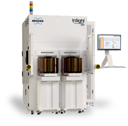
Image Credit: Bruker Nano Surfaces and Metrology
Built with Semiconductor Metrology Expertise
Experience, Service, and Support
Bruker’s automated atomic force microscopes (AAFMs) have been a trusted choice for semiconductor fabs around the world. From the first fully automated 200 mm fab AFM to the latest InSight 300, Bruker has delivered patented innovations that support the ongoing advancement of next-generation semiconductor technologies.
Bruker is committed to maximizing tool uptime and productivity, offering:
- A global service and support team known for resolving issues on the first attempt
- Strategically located service depots to ensure fast access to parts
- Flexible service programs tailored to specific support needs
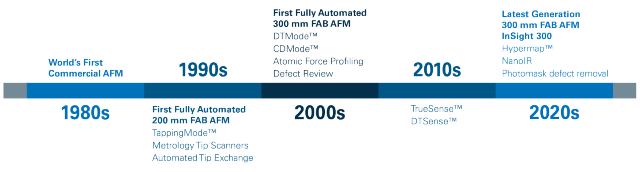
Bruker's semiconductor metrology innovation timeline. Image Credit: Bruker Nano Surfaces and Metrology
Specialized Probes
Application-specific probes offer the most reliable and precise method for characterizing advanced nodes. Bruker remains the only AFM manufacturer that owns and operates a dedicated nanofabrication facility for probes, continually developing new designs tailored to specific applications.
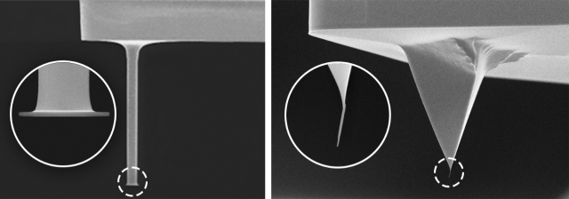
(left) CDR1000-10UM probe for sidewall imaging. (right) BNT-500-12 probe with a >500 nm long EBD spike, suitable for a multitude of applications. Image Credit: Bruker Nano Surfaces and Metrology
Focused on Production
Superior Capabilities
The InSight 300 provides stable, artifact-free data that is NIST-traceable. Leveraging built-in expertise, it performs precise and repeatable tasks, including:
- Depth metrology
- Roughness metrology
- Automatic defect review
- Surface profiling
- Sidewall profiling
- Hybrid bonding
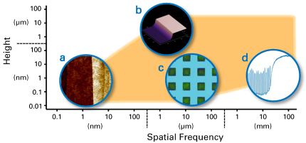
Map representing field of view, spatial frequencies, and height ranges covered by Insight 300’s AFM and profiling capabilities. Examples shown are (a) atomic steps on 2D material, (b) 10 µm step height, (c) 100 µm bond pad metrology scan, and (d) >20 mm profile scan. Image Credit: Bruker Nano Surfaces and Metrology
Application-Specific Modes
Tailored operating modes enable maximum throughput without compromising metrology accuracy. The InSight 300 includes Bruker’s patented modes designed for specific applications, such as surface profiling, depth measurement of high aspect ratio features (DTMode), roughness (TrueSense®), and sidewall roughness and angle (CDMode).

Bruker’s specialized application-dedicated operating modes: TrueSense®, Profiling, DTMode, and CDMode. Image Credit: Bruker Nano Surfaces and Metrology
Automatic Tip Management
Bruker’s TipX technology on the InSight 300 delivers full probe automation and quality assurance for HVM. Probes are automatically loaded and qualified to meet recipe specifications. Vacuum-based holding ensures secure placement, broad probe selection flexibility, and reduced overall probe costs.
(left) Automatic probe shape qualification. (right) Probe cassette with a 25-probe capacity. Image Credit: Bruker Nano Surfaces and Metrology
Verified Performance
Throughout development and production, performance is continually validated through long-term stability, linearity, and accuracy testing.
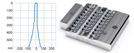
The InSight 300’s AFM scanner, featuring a scanning-tip design, is engineered to meet modern nanoscale metrology demands, with less than ±1 nm of out-of-plane motion across a 105 µm2 scan area, up to 18 µm of Z range, and the integration of a long-range profiling stage.
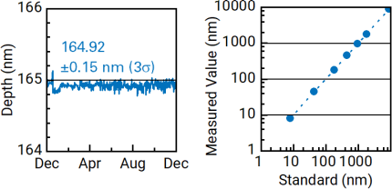
(left) Statistical process control chart showing sub-nanometer long-term stability. (right) Step height on VLSI reference samples showing high accuracy and linearity. Image Credit: Bruker Nano Surfaces and Metrology
Versatile Optics
The InSight 300’s integrated optics enable fast recipe site setup and straightforward navigation to areas of interest. A dual-channel, tip-centric objective combined with a third offset objective delivers exceptional optical resolution, all while maintaining maximum field of view.
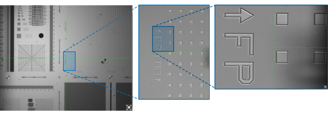
Field of view and resolution for InSight 300’s integrated optics, illustrated on a MetroBoost FP100 reference structure. Image Credit: Bruker Nano Surfaces and Metrology
Modern GUI
The InSight 300 is designed for ease of use. Its operator-friendly graphical user interface (GUI) enables technicians and engineers to efficiently create and manage recipes, including recipe-controlled tip management and resource tracking. To keep tools running during development, recipes can also be created and edited off-tool.
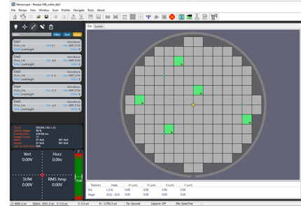
Automated wafer map generation and recipe wizard. Image Credit: Bruker Nano Surfaces and Metrology
Applications
Optimized for the Applications
Roughness Metrology
InSight 300’s best-in-class noise levels enable sub-angstrom surface roughness control, supporting quantitative roughness measurements below 100 pm RMS. Even at MAM times of ~1 min/site, the system delivers reliable data with strong repeatability (e.g., 3σ < 10 pm for smooth surfaces with RMS roughness < 1 nm) and consistent tip-to-tip performance.
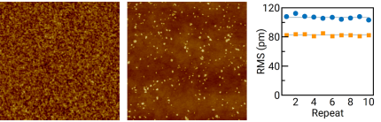
(left) Ultrasmooth Si (85 pm RMS, 1 nm Z scale, 1x1 µm scan). (middle) Post-CMP ILD area with 0.42 nm RMS (8 nm Z scale, 3 × 3 µm scan). (right) High-throughput roughness metrology repeatability result on two Si wafers with 106 pm RMS and 83 pm RMS, 3 σ<5 pm. Acquired at <1 min MAM time. Image Credit: Bruker Nano Surfaces and Metrology
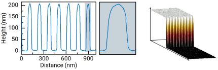
Depth Metrology
Bruker’s proprietary deep trench mode (DTMode) is specifically designed for measuring narrow trenches and vias with depths from tens of nanometers to over 10 µm.
Paired with application-specific high aspect ratio tips, DTMode meets the depth metrology demands of HVM etch process control - delivering results with MAM times under 10 seconds.
(left) DTMode scan and (right) section profiles of a dense array of vias (depths 80 to 100 nm), enabling within-wafer process variation studies. Image Credit: Bruker Nano Surfaces and Metrology
Sidewall Profiling
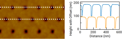
Sidewall angle (SWA) and sidewall roughness (SWR) are key parameters affecting device and IC performance. Accurate measurement of these dimensions with AFM requires a mode purpose-built for this metrology, since scanner tilting can introduce significant TMU.
Bruker’s critical dimension scan mode (CDMode) is the industry’s only true CD-AFM solution. It offers the lowest TMU available, along with unmatched accuracy and repeatability.
(left) CDMode characterizes a line/space pattern with 150 nm pitch for (middle) high-resolution SWA, and (right) line edge roughness. Image Credit: Bruker Nano Surfaces and Metrology
Automatic Defect Review
AFM-based defect review offers a non-destructive alternative to traditional methods such as SEM or EDX, and uniquely enables adhesion measurement to support more accurate defect classification.
InSight 300 supports fully automated, recipe-driven defect review with KLARF compatibility. Productivity is maximized through fast recipe creation (under five minutes) and automated bare wafer registration, enabling throughput of tens of defects per hour.
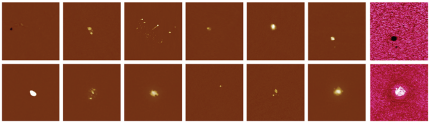
High-resolution height scans of various nanometer-scale defects (2x2 µm scans), and simultaneously acquired adhesion measurements (final two images, in pink) further aiding defect classification. Image Credit: Bruker Nano Surfaces and Metrology
Surface Profiling
The InSight 300 can be configured for best-in-class surface profiling. Its advanced non-contact linear stage enables measurements over distances up to 50 mm at speeds reaching 1 mm/s, with precise control of both local and long-range planarity.
Profiling applications include step height measurement, bevel edge rounding, and post-CMP analysis of dishing and erosion.
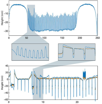
Post-CMP profiling (2 nm data spacing) with high repeatability for both dishing (3 σ = 0.14 nm) and erosion metrology (3 σ = 0.32 nm). Image Credit: Bruker Nano Surfaces and Metrology
Hybrid Bonding
The Insight 300 automated AFM can be applied in the most current hybrid bonding technology nodes, providing high-resolution imaging and dedicated analysis for critical bond pad metrology, as well as automated bevel edge metrology for hybrid bonding.
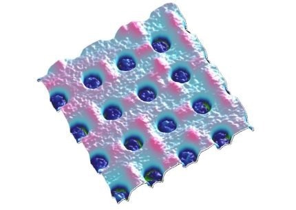
Cu/ILD pattern post-CMP revealing critical roughness and recess depth information for the hybrid bonding process. Image Credit: Bruker Nano Surfaces and Metrology
Specifications
InSight 300 Automation Specifications
Each semiconductor fab and wafer manufacturing facility faces its own unique requirements and challenges. The listed product specifications and offerings are a starting point for discussions with our experts to explore how InSight 300’s capabilities can best support your needs.
Source: Bruker Nano Surfaces and Metrology
| . |
. |
| Fab Automation |
SECS/GEM Host Automation Interface, E84 PI/O AMHS support |
| SEMI Standards E4, E5, E30, E37 & E37.1, E39 & E39.1, E40, E87 & E87.1, E90, E94, E116 & E116.1 |
| Regulatory Compliance: CE, UKCA, KC, SEMI S2/S8, F47, 21 CFR 1040.10, 21 CFR 1020.40 |
| Tip Handling |
Automated Tip Management and Tip Exchange |
| Tip Capacity: 4 Cassettes, 25 Tips each |