The Hysitron PI Envision SEM PicoIndenter delivers high-performance nanomechanical testing capabilities in a compact, easily upgradable format that integrates seamlessly into a wide range of microscopy setups.
With best-in-class control and over fifty interchangeable tips, PI Envision enables precise measurement of mechanical properties across a broad spectrum of materials - from soft polymers to hard ceramics.
The system offers sub-nanometer resolution in both force and displacement, and supports advanced testing modes, including high-throughput nanoindentation, mechanical property mapping, nanotribology, and high-temperature testing.
Thanks to its modular architecture, PI Envision is ideal for both routine workflows and specialized research. It provides the flexibility needed to adapt to evolving research programs and multi-user environments that demand high data quality, experimental versatility, and long-term scalability.
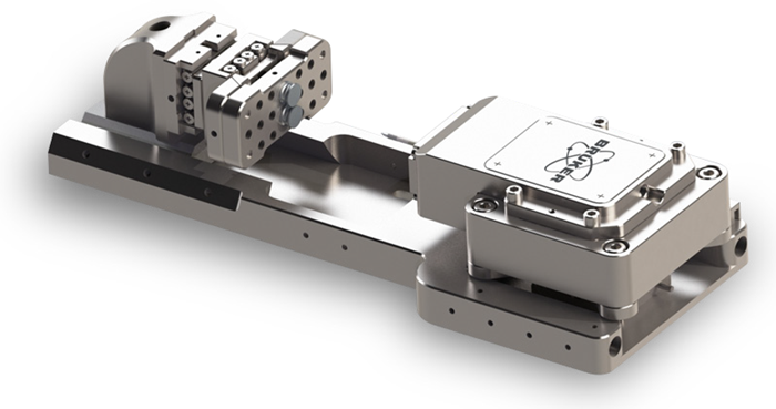
Image Credit: Bruker Nano Surfaces and Metrology
Hysitron PI Envision Delivers:
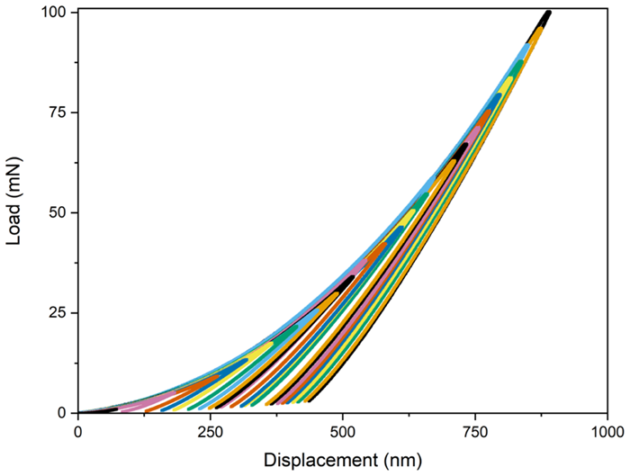
Load-displacement curve with high-load transducer option. Image Credit: Bruker Nano Surfaces and Metrology
- Achieve sub-nanometer precision with up to 250 mN force capacity and 100 µm displacement for accurate characterization of a wide range of materials
- Expand capabilities with advanced upgrades for nanotribology, mechanical property mapping, and high-temperature testing up to 800 °C
- Encoded stage control and a 78 kHz feedback rate deliver fast, repeatable results across indentation, compression, tension, and fatigue testing
Intuitive Operation for a Wide Range of Testing Modes
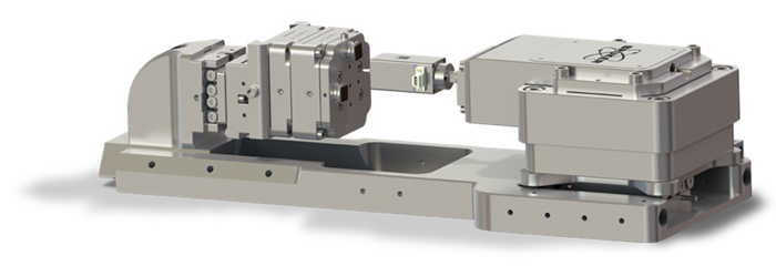
Image Credit: Bruker Nano Surfaces and Metrology
In-situ scratch testing using the nanoScratch module. Image Credit: Bruker Nano Surfaces and Metrology
PI Envision utilizes Hysitron’s core transducer technology for consistent and dependable nanoindentation results. Designed to optimize usability, throughput, and overall performance, this PicoIndenter includes features that enhance both experimental flexibility and operational efficiency:
- A large tip-to-mount standoff distance enables room-temperature testing of samples up to 25 mm thick
- An encoded stage ensures accurate and repeatable sample positioning within an extended 12 × 12 mm travel range
- Dual sample mounts improve workflow efficiency by reducing manual exchanges and supporting flexible experiment setups
Exceptional Value with an Easy Path to Future Upgradability
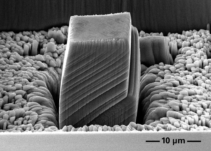
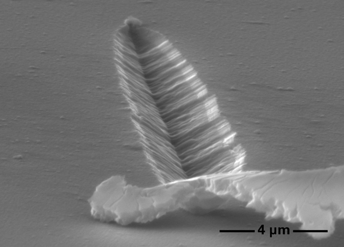
Micropillar compression with PI Envision. Image Credit: Bruker Nano Surfaces and Metrology
PI Envision has standard force capabilities of up to 10 mN and a displacement range of 1 nm to 5 µm. The device offers a wide range of conventional and optional testing modes, including nanoindentation, compression, bending, direct-pull tension, push-to-pull tension, nanoDynamic, property mapping, and electrical characterization.
System configurations can sustain loads up to 250 mN and have a displacement range of 1 nm to 100 µm, enhancing performance. These setups provide additional testing modules, such as high-temperature testing at 800 °C and nanotribological characterization.
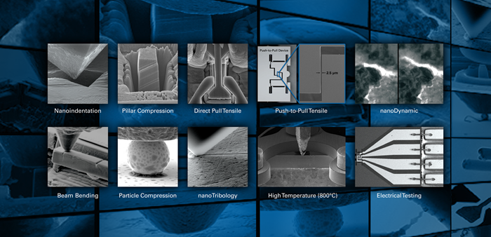
Image Credit: Bruker Nano Surfaces and Metrology
Hysitron PI Envision Specifications
Source: Bruker Nano Surfaces and Metrology
| |
| Max Force (transducer dependent) |
10 mN; 250 mN |
| Force Noise Floor (inside an SEM, 60 Hz) |
<0.4 μN |
Force Noise Floor (in ideal environment,
60 Hz, 10 mN transducer) |
<50 nN |
| Maximum Displacement |
5 μm; 30 μm; 100 μm |
Displacement Noise Floor
(inside an SEM, 60 Hz) |
<1 nm |
| Displacement Noise Floor (ideal environment, 60 Hz, 10 mN transducer) |
<0.1 nm |
| Machine Stiffness |
0.7 × 10⁶ N/m |
| Sample Positioning Range and Sensitivity |
12 mm × 12 mm × 16 mm (indentation axis); 1 nm encoder |
| System Size (base system, excluding SEM stage connecting adapter) |
55 mm × 32 mm × 191 mm (W × H × L); 460 g |
| Multi-Sample Mount |
Yes |
| Automated Indentation with Stage |
Large area: (>1 mm × >1 mm), no stitching |
| Tip Options |
Over 50 available, including diamond, sapphire, vanadium carbide, boron nitride, tungsten, and steel |
Hysitron PI Envision Modes and Capabilities
Source: Bruker Nano Surfaces and Metrology
| |
| Nanoindentation Testing |
Supports load-controlled, displacement-controlled, and open-loop for fundamental mechanical characterization |
| Compression Testing |
Enables intrinsic displacement-controlled testing of micropillars, nanoparticles, and other small-scale structures |
| Direct-Pull Tensile Testing |
Employs a gripper probe to apply stable, uniaxial tensile loads for accurate material response |
| Push-to-Pull (PTP) Tensile Testing |
Uniquely simplifies tensile testing of nanostructures such as nanotubes, nanofibers, nanowires, and thin films (patented by Bruker) |
| Electrical PTP Tensile Testing |
Enhances PTP testing with integrated four-point electrical measurements to study electromechanical coupling |
| nanoScratch Testing |
Simultaneously captures normal and lateral forces to evaluate friction, interfacial strength, and adhesion - ideal for semiconductor materials and coatings |
| Electrical Characterization |
Monitors changes in electrical properties during mechanical deformation; applicable to piezoelectric and other functional materials |
| High-Temperature Heating |
Enables mechanical testing - quasi-static, dynamic, and mapping - at elevated temperatures up to 800 °C |
| Property Mapping |
Rapidly generates high-spatial-resolution quantitative mechanical property maps |
| nanoDynamic Testing |
Applies oscillatory forces to continuously evaluate viscoelastic and fatigue properties at room and elevated temperatures |