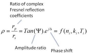
The physical properties of the layer structure being analyzed are included in the measured ellipsometric parameters (Ψ and Δ). This information exhibits the layer thickness and refractive index concerning the fundamental equation of ellipsometry.
As the equation is extremely nonlinear and transcendental, it is necessary to solve the equation by utilizing numerical techniques on a model-based perspective. The layer structure is analyzed in terms of the thickness and optical functions of the model during the technique.
The relative phase shift is calculated and placed in comparison with measured quantities via a numerical regression process.
Optical Modeling
A loose optical model of the structure must be deciphered whilst the numerical regression process is happening. A substrate is usually approximated by utilizing a semi-infinite material which has known optical characteristics and is thick.
Parametric functions are frequently utilized to outline the spectral absorption and dispersion of each layer. Basic empirical formulas or more multifaceted definitions can be used depending on the material.
Where a parametric function has happened, for instance in the case of the Cauchy law, more than a few parameter values are used to parametrize the dispersion. In this instance, A, B and C, are known to be useful parameters when regression has occurred.
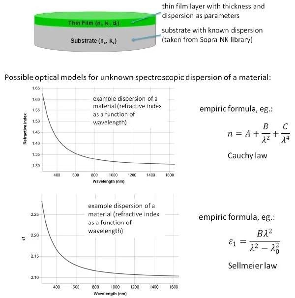
Image Credit: Semilab Semiconductor Physics Laboratory
The refractive index can be measured as a function of wavelength if the parameters are gathered at the end of the regression process. The Sellmeier model is another option for modeling the dielectric function, whereas the Cauchy law is an empirical formula.
This model is based on a zero linewidth Lorentzian absorption peak found away from the range of measurement at oscillator strength B and peak position λ0. So, the film has no optical absorption within the wavelength range being measured.
Its hyperbolic-shape can be equal to those gathered when utilizing the Cauchy model. The advantage of using the Sellmeier model is that it can be combined easily with alternative dispersion formulas which are refined for complex dielectric functions such as Drude, Gauss, or Lorentz.
It can capture more than one Sellmeier peak in a single model and is an applicable model for wider wavelength range modeling.
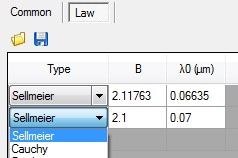
SEA software selection of dispersion law types in Structure tab. Image Credit: Semilab Semiconductor Physics Laboratory
Performance of Dielectric Film Measurement
The range of sensitivity for the measurement of optically transparent films can differ from several tens of micrometers to sub-nanometers. The simulation result clearly exhibits sub-nm sensitivity, for instance, for SiO2 covered Si substrate in the Δ curve above 600 nm wavelength.
The higher limit of establishing dielectric film thickness is dependent on the maximum wavelength resolution and range created for the spectroscopic ellipsometer instrument utilized.
The refractive index variation between the thin film coating and the substrate is reduced dramatically in the context of the SiO2 and Si sample structure when glass substrate is employed.
For this reason SiO2 or glass measurements require instruments which are of a high sensitivity and can optically distinguish between two similar dielectrics.
It is possible to measure SiO2 thickness on glass sheets even where the thickness range is as small as <50 nm by using Semilab’s rotating compensator ellipsometer.
This method of application is more relevant in recent times for the flat-panel display industry where the oxide coating acts as an initial buffer layer, and has to be deposited comparably across the several m2 area panels of glass.
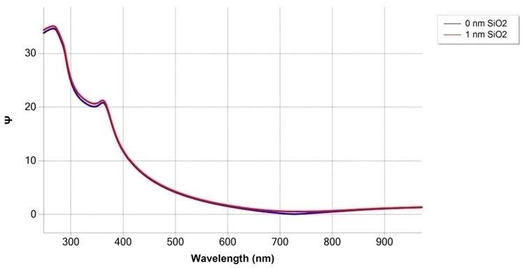
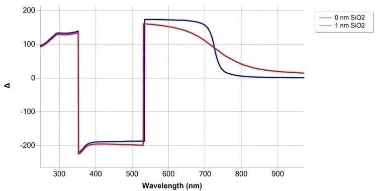
Simulation of SiO2/Si measurement at 75° angle of incidence, with and without 1 nm SiO2 film. Image Credit: Semilab Semiconductor Physics Laboratory
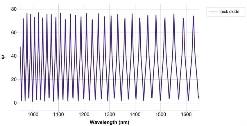
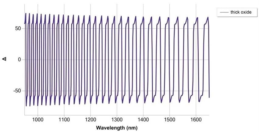
Simulation of SiO2/Si measurement at 75° angle of incidence, with thickness 30 μm with NIR fast detection spectrograph. Image Credit: Semilab Semiconductor Physics Laboratory
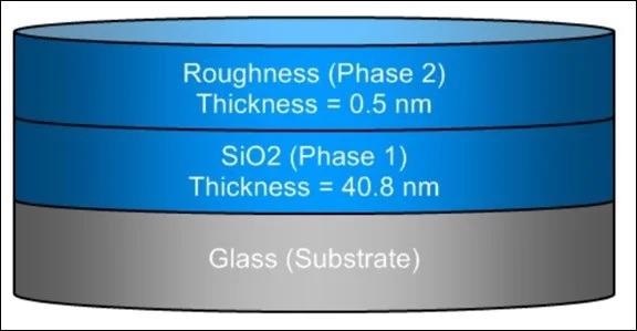
Optical model result output for the sample structure of thin SiO2/glass. Image Credit: Semilab Semiconductor Physics Laboratory
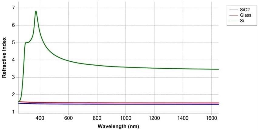
Refractive index difference for SiO2 layer vs. glass or Si substrates. Image Credit: Semilab Semiconductor Physics Laboratory
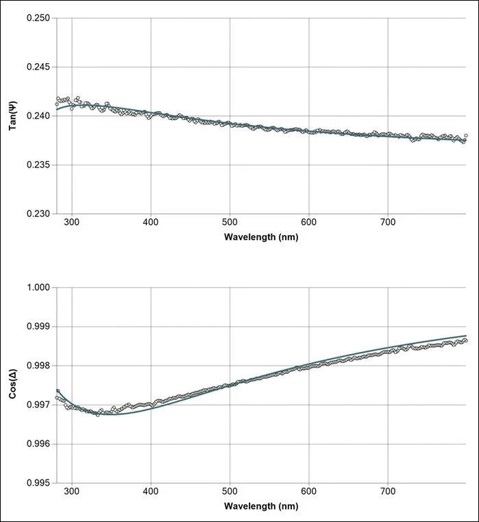
Measured and fitted spectrum of thin SiO2/glass sample at 65° angle of incidence. Image Credit: Semilab Semiconductor Physics Laboratory

This information has been sourced, reviewed and adapted from materials provided by Semilab Semiconductor Physics Laboratory.
For more information on this source, please visit Semilab Semiconductor Physics Laboratory.