The majority of semiconductor devices are made up of heterostructures, which are stacked layers of distinctive materials deposited by utilizing distinctive methods. These layers have a thickness in the range of micrometers down to nearly singular atomic thickness.
At layer interfaces, the electronic configuration plays a key part in the accurate operation of an electronic device. It is possible to simulate the electronic characteristics of such interfaces but a number of physical influences from the deposition process and layer interactions have an effect on the interface in a specific and often unpredictable manner.
This article outlines a robust way of carrying out an in situ analysis of heterostructure interfaces by using an organic solar cell structure as an example. The method and the study discussed in this article were developed and performed by Saive et al.1
The electrical characterization of interfaces has been carried out using Scanning Kelvin Probe Force Microscopy (SKPM). The SKPM method is similar to a traditional Kelvin probing system in that it provides information related to the work function (chemical potential) difference between the sample surface and a sensing tip.
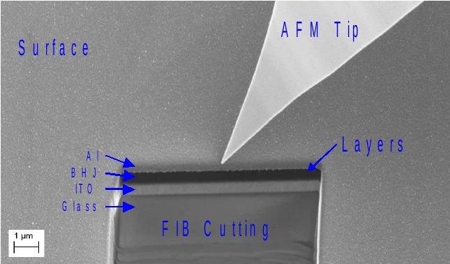
Sample after preparation by focused ion beam (FIB). Image Credit: Semilab Semiconductor Physics Laboratory
In the case of SKPM, an atomic force microscope (AFM) tip is employed as a Kelvin probe sensor, which allows the measurement of changes in work function with extremely high lateral resolution, and in certain cases, down to the atomic level.
The electronic configuration such as carrier type and density, the inherent potential of a material and an ultimately applied electrical potential influence the work function. An SKPM measurement on the cross-section of a heterostructure results in absolute measurements of differences in work function between the different layers.
This also enables the direct measurement of the drop in voltage between the different layers upon applying an external voltage over the heterostructure. These semiconductors have to be enclosed in airtight containers as the surface of an organic semiconductor is highly sensitive to air exposure.
The exposed surfaces must be protected from air contamination for high resolution electrical characterization. The combination of the Carl Zeiss AURIGA crossbeam workstation and the Carl Zeiss AFM option for MERLIN permits the solar cell to be prepared and investigated without the prepared structure being exposed to air.
The high capability zoom of the SEM ensures that the AFM tip is navigated directly to the region of interest with precision so that information regarding the topographical, mechanical, electrical and magnetic properties of the surface can be collected at nanoscale resolution.
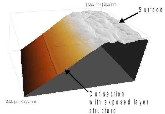
AFM micrograph showing the 3D topography of the cut-out section. Image Credit: Semilab Semiconductor Physics Laboratory
SEM-AFM
When compared to the two systems, a combined SEM-AFM has a number of benefits as stand-alone. The system supplies innovative possibilities for the measurement of surfaces and nanostructures.
The SEM and AFM combination allows the accurate positioning of the AFM tip. The AFM supplies precise information related to the topographical, electrical and mechanical properties of the surface.
Image Credit: Semilab Semiconductor Physics Laboratory
Applications
- Analysis of surface properties like:
- Conductivity of the surface
- Chemical surface potential by Kelvin Probe Force Microscopy (KPFM)
- Magnetic force on the surface of the sample
- Electrical and topographical properties
- Potential difference between the two electrode materials
- Graphene and other 2D materials
- Potential distribution along the layer structure of an SMD capacitor
- Characterization of:
- Sustainable energy production
- Energy storage
- Heterogenic structures of nanosized devices and functional structures in semiconductor
Hardware Integration
The method used to achieve a combined SEM-SPM system is dependent on the integration of a vacuum compatible SPM into current SEM systems. This combination was selected to attain the highest performance and usability of the system.
Another benefit of this approach is that it is possible to optimize current SEM systems to a combined SEM-SPM system. In both instances, the function of the SEM will not be limited, allowing combined SEM/SPM measurements.
The SPM is designed like a sample scanner for integration. As the tip and the beam are not moved against each other, this design enables the highest precision alignment of the SPM tip and the electron beam.
This permits unknown probabilities of combined measurements even at the time of SPM scanning. The framework also has the ability to realize the highest performance in terms of resolution and frame rate.
The scan unit itself is the next advancement step of the SemiLab STM scanner, famous over the last few decades for high reliability and stability. The claim of the design for high resolution is clearly evident, with a possible sample size of 10 mm and a scan volume of 9 µm × 9 µm × 1 µm.
Electronic components like the laser diode, detector and preamplifier are located inside the vacuum chamber in hermetically encapsulated compartments. The exchange of the cantilever and the sample, in addition to the alignment of the laser path, can be performed without breaking the vacuum.
The SPM tip can be positioned to the area of interest and with the help of a remote control, the SPM can be positioned with respect to the SEM. By making small alterations to the SPM, a UHV-compatible version can be availed.
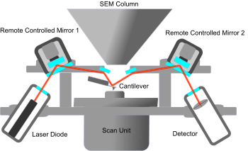
Image Credit: Semilab Semiconductor Physics Laboratory
Software Integration
The operating software dictates the grade of functionality of highly complex scientific instruments like the SEM-AFM. In order to realize the seamless integration of the techniques, a single-software user interface is needed.
The open design of the from Semilab permits the integration of a self-designed SEM operating software. The operator can thus control both the systems from a single platform and the same software without the requirement to click through a network of windows and tabs.
The view on all settings and image data of both methods is unblocked and accessible. The software has been created for the highest throughput and workflow.
At the same time, program functions like the DME Automator provide access to all functions of the SEM-AFM system, allowing user-designed advanced measurement routines to be designed and executed.
In order to acquire comparable data from different regions of the sample, automatically running measurement routines can be created. The ScanTool™ software is used to examine image data from SEM and SPM.
Standard analyzing tools or more specialized or advanced analysis procedures can be performed by the company based on customer demand, through the ‘DME Automator’ or ‘DME Image Calculator.’
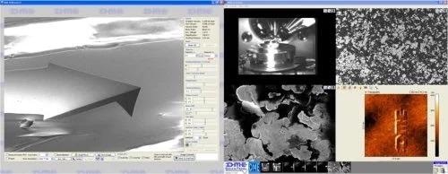
Image Credit: Semilab Semiconductor Physics Laboratory
Features
- Single-software interface for both SEM and AFM components.
- The SEM-AFM system is based on the DME UHV AFM and the Carl Zeiss Auriga® Crossbeam Workstation.
- Highly stable scan unit developed for 3D single-atomic resolution.
- Ability to update prevalent Auriga® SEMs to BRR functionality by simple door exchange
- SEM viewing angle of 0°- 85° while maintaining a minimum SEM working distance of 5 mm.
- The crossbeam point of SEM and FIB lies at the cantilever tip. The design as a sample scanner permits combination measurements of all three methods at precisely the same point on the sample and in space.
- Scanner specification: scan range (x,y,z) 10 µm × 10 µm × 1 µm, real resolution subatomic in all three dimensions.
- Ability to reach the cantilever tip and the sample by FIB in 0° and 54° position, in situ tip sharpening by FIB supported
- Automatic laser/detector alignment on cantilever change
- Supports easy exchange between AFM and standard Auriga® functionality by user-exchangeable SEM door
- Common data storage of AFM and SEM images
- Supports all common AFM operation modes
- Unlimited functionality through the utilization of all standard AFM cantilevers, without the requirement for active probes
References
- Rebecca Saive, Michael Scherer, Christian Mueller, Dominik Daume, Janusz Schinke, Michael Kroeger, Wolfgang Kowalsky, Imaging the electric potential within organic solar cells, Advanced Functional Materials Volume 23, Issue 47, December 2013, Pages 5854-5860.

This information has been sourced, reviewed and adapted from materials provided by Semilab Semiconductor Physics Laboratory.
For more information on this source, please visit Semilab Semiconductor Physics Laboratory.