Right from food containers to photovoltaics, thin films and coatings play a key role in everything. For such varied requirements to be fulfilled, they are created from every class of material and by several processes such as chemical and physical vapor deposition methods, sol-gel processing, and atomic layer deposition.1
The main step in coming up with any new film is defining its surface structure and physical properties, albeit in engineering commercial products (Figure 1) or pursuing basic materials science (Figure 2).The inherent dimensions of films (grain, thickness, domain sizes, etc.) make it crucial to define them on sub-nanometer to micrometer length scales. AFM is a strong tool that has been specifically developed for this purpose for various reasons. For example, it holds much greater spatial resolution compared to other stylus or optical-based techniques.4
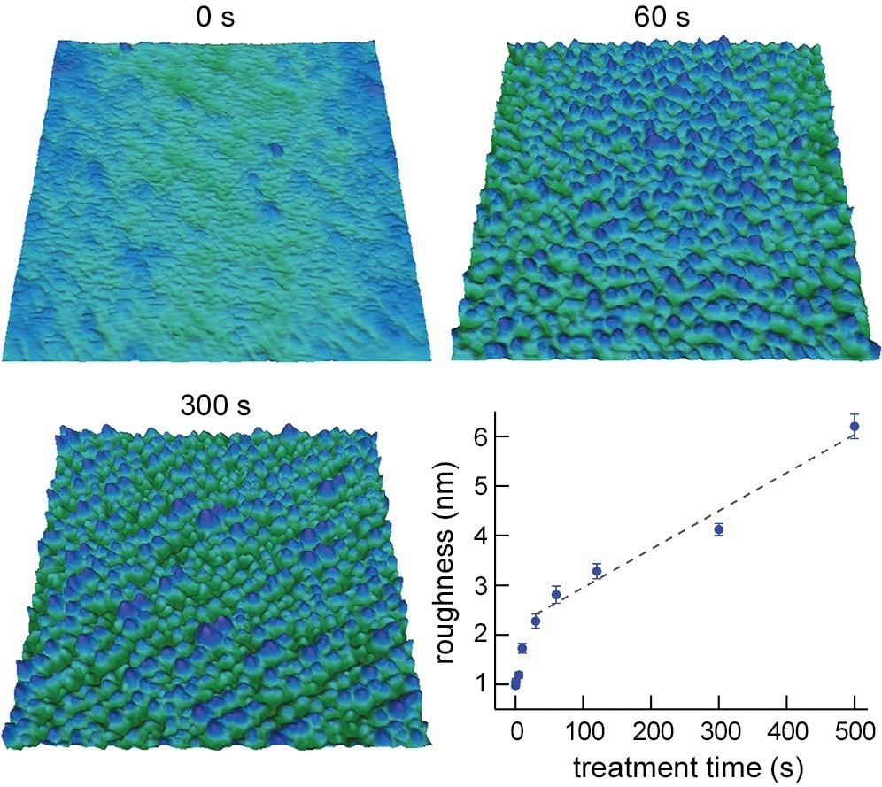
Figure 1. Oxygen plasma treatment of polyethylene terephthalate (PET) films. PET fibers coated with a conducting polymer such as polypyrrole could be used in “smart” electronic textiles. However, achieving good coating-to-fiber adhesion remains a key challenge. Images of PET films exposed to oxygen plasma show that RMS surface roughness increased with exposure time. Films processed longer than 60 seconds displayed surface etching and uniform nanoscale features. The graph reveals a linear dependence of roughness on treatment time after ~30 seconds. Combined with data on surface chemistry, the results can be used to optimize treatment parameters for improved coating adhesion and conductivity. Scan size 1 μm; height scale 35 nm. Imaged with the Cypher S AFM. Image Credit: Adapted from Mehmood et al.2
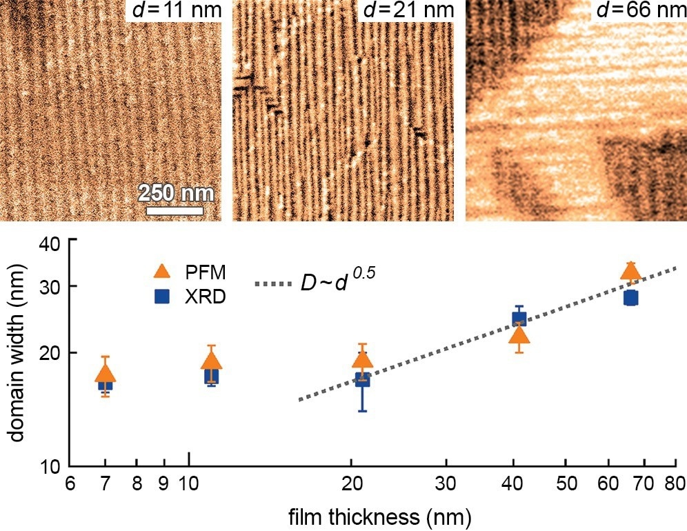
Figure 2. Strain effects in ferroelectric NaNbO3 (NNO) films grown on TbScO3 (TSO) substrates with metal organic chemical vapor deposition (MOCVD). Growth of epitaxial NNO on TSO results in significant anisotropic misfit strain. Understanding relations between strain, crystal structure, and ferroelectric response will enable finetuning of film properties. The lateral piezoresponse force microscopy (PFM) image on a film with thickness d = 11 nm reveals a strong in-plane piezoresponse with highly ordered domains (vertical stripes). For a thicker film (d = 21 nm), distortions in the alignment appear. For an even thicker film (d = 66 nm), 90º domains (horizontally striped regions) are observed, indicating a 1D to 2D domain pattern transformation. The graph shows values for the lateral piezoelectric domain width D obtained by PFM and x-ray diffraction (XRD). The dependence of D on d changes from approximately constant to the predicted D ∝ d0.5 (dotted line) at d ≈ 20 nm, where the 1D to 2D transformation occurs. Acquired on the MFP-3D AFM. Image Credit: Adapted from Duk et al.3
The inherent dimensions of films (grain, thickness, domain sizes, etc.) make it crucial to define them on sub-nanometer to micrometer length scales. AFM is a strong tool that has been specifically developed for this purpose for various reasons. For example, it holds much greater spatial resolution compared to other stylus or optical-based techniques.4
There is a need for samples not to be electrically conducting or optically reflective, thereby enabling access to virtually any film. Also, AFMs offer complementary data to electron microscopes, like precise 3D surface profiles.
It also offers a highly adaptable operating surrounding for work at both ambient and non-ambient atmospheres and temperatures.
In this context, the extensive features of Asylum Research AFMs for thin-film characterization have been explained and examples over a range of applications have been displayed. With AFMs that are available at present, it is possible to quantify surface roughness more precisely, rapidly, and easily compared to ever before.
A broader range available for automated routines and built-in analysis tools implies greater productivity and higher user-friendliness. Furthermore, research and instrumentation advances have made a range of AFM modes for quantifying nanoscale film functionality such as magnetic, electrical, and mechanical responses.
Imaging Topography
A surface structure like texture and roughness is frequently associated with the behavior of the film. For example, grain size impacts electromigration in copper interlinks, while the microstructure of diamond-like carbon coatings tends to impact friction in cutting tools.
Furthermore, roughness identifies wettability in biocompatibility coatings for medical implants, and nanopatterning to regulate roughness enhances the efficiency of LEDs.
Quantifying surface roughness at the time of the product development cycle has the potential to offer process control metrics and disclose structure-property relations. Also, measurements can be utilized to comprehend the impacts of post-deposition treatments (heat, polishing, plasma, etc.) and clarify product failure modes.
The availability of the three-dimensional AFM images of topography (height) provides nanoscale information on film structure such as defects, roughness, amorphous and crystalline phases, and nucleation and growth modes.
Generally, topographic imaging is executed in tapping mode. In this context, the AFM cantilever oscillates next to its resonance frequency, and the probe tip only touches the sample at the time of the part of the oscillation cycle.
In comparison to contact mode, the much tender lateral and vertical tip-sample forces in tapping mode decrease damage to both the sample and the tip. The high spatial resolution of the tapping mode emerges from ultrasharp tips and the small tip-sample contact area so that even atomic and crystal structures can be resolved (Figures 3 and 4).
The precision of AFM topography measurements relies on the spatial resolution in both the vertical (Z) and lateral (XY) directions. In the Z direction, the resolution has been restricted primarily by instrument noise. Factors like random electrical fluctuations and mechanical vibrations establish variations in the height signal.
Height features smaller than these changes cannot be resolved in a meaningful manner. Also, the linearity of the Z piezo could affect precision, particularly on samples with greater roughness. The lateral resolution has been primarily identified by the size of the AFM cantilever tip and its effect on the tip-sample contact area.
Normally, the tip radius is <10 nm when new, so a tip-sample contact radius of <1 nm is general in tapping mode. But gradual tip wear will affect both the feasible lateral resolution and measurement repeatability or accuracy.
It is possible to avoid tip blunting if the AFM has a flexible mechanical Z-axis. By rapidly adapting the cantilever base in reaction to surface height variations, the Z-axis prevents the tip from employing bigger forces compared to what is intended, thereby safeguarding the tip from damage.
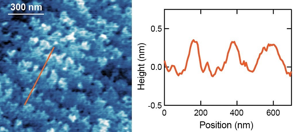
Figure 3. Topography imaging of atomically flat strontium vanadate (SVO). The epitaxial film was grown by pulsed electron-beam deposition and was ~6.5 nm thick. SVO has potential applications in electronic switching and sensing, and recent advances in synthesis techniques enable growth of low-dimensional, ultrathin films with improved functionality. The image was acquired with the Cypher S AFM and demonstrates its superb Z resolution. Height scale 0.9 nm. The section across the line in the image shows the atomically flat nature of the film, with step-terrace structures high corresponding to the lattice spacing of one unit cell. Image Credit: Adapted from Gu et al.5
One problem in topography measurements is image drift, which has a big impact on repeatability and fidelity. Thermal variations are known as the primary source of drift, for instance, as a result of fluctuations in room temperature.
Such changes can make the AFM components extend and contract so that the comparative position between the cantilever and the samples gradually alters. Thermal drift can be decreased greatly by cautious instrument design or by actively regulating AFM temperature.
In addition to the enhanced technical specifications like spatial resolution, the past few years have seen other upgrades to Asylum Research AFMs. Automated setup tools and various data analysis routines have been added for efficient operation.
The considerable increase in image acquisition speed should also be noted. Quicker scanning increases throughput, for example, to evaluate film uniformity by imaging various sample regions. High scan rates are possible with the help of AFMs like the Asylum Research Cypher which utilizes smaller cantilevers with greater resonant frequencies.
Furthermore, small cantilevers offer noise and resolution advantages, and could better solve and regulate very low (sub-piconewton) forces. Such benefits imply that imaging features like single-point atomic defects and the DNA double helix are not just possible but commonplace on Cypher AFMs.
Asylum AFMs for Topographic Imaging
- The newest generation of position sensors, with noise levels as low as 35 pm in Z (Infinity) and 60 pm in X and Y (Cypher), are found in the Cypher and MFP-3D InfinityTM AFMs. For precise and consistent scanning motion, closed-loop scanners are a standard feature on all Asylum AFMs. This removes image distortions and makes it possible to zoom in and offset with high precision on particular scan areas.
- On Cypher AFMs, line scan rates up to 40 Hz are routinely possible due to small cantilevers (<10 µm long), which results in a 5- to 10-second turnaround time for a complete 256 × 256 pixel image.
- Even when imaging atomically flat samples, Cypher AFMs can be used in most labs without the need for vibration isolation apparatus. They have an integrated acoustic enclosure and were made with the highest mechanical stability in mind. These characteristics reduce thermal drift by 10× compared to less sophisticated AFMs and make them almost impervious to common environmental noise.
- GetStartedTM automates the optimization of imaging parameters, accelerating and simplifying tapping mode. Predictive algorithms are available on MFP-3D Infinity and Cypher AFMs, guaranteeing that high-quality data is obtained from the first scan line. These algorithms set parameters before the tip even touches the sample.
- Setting up Cypher AFMs is significantly faster with SpotOnTM automated laser alignment. The fully motorized stages align the laser spot on the cantilever and center the photodetector with just the click of a mouse on the desired position.
Analyzing Roughness
Roughness parameters outline the complicated 3D information of topography images, for example, for samples to be compared. There are several roughness parameters,4,7 but just three primary types: spacing, hybrid, and amplitude.
Amplitude parameters define the surface depending on its Z variations, while spacing parameters explain XY variations. Hybrid parameters like slope and curvature explain changes in X, Y, and Z.
Surface roughness is most commonly described by amplitude parameters such as the average deviation Ra or Adev, the root mean square RRMS, and the standard deviation Rq or Sdev.
Such parameters have units of length, with greater values signifying bigger height variation. Since they do not differentiate between valleys and peaks or the spacing of features, parameters can exhibit the same value for samples with highly different textures. RRMS and Sdev are more sensitive compared Adev to occasional highs and lows.
However, both RRMS and Sdev explain the spread or dispersion in height changes, but Sdev is normally smaller compared to RRMS since it does not include the average height. Figure 4 displays a systematic analysis of topography images to define multiferroic films.
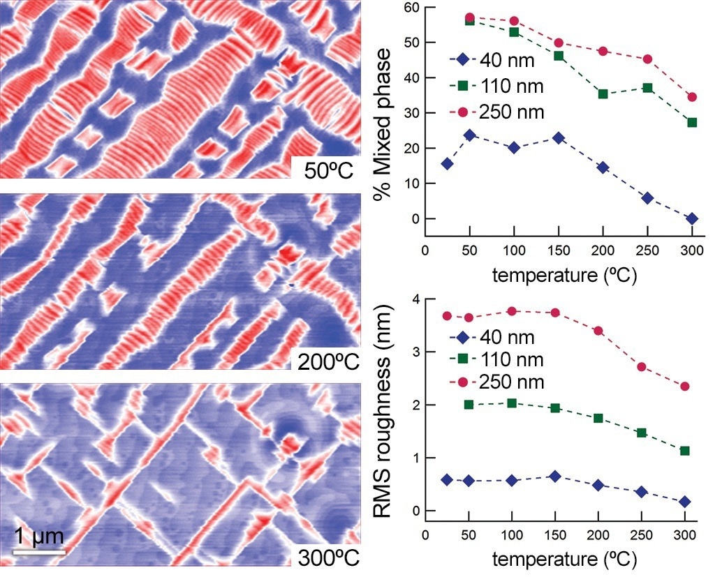
Figure 4. Temperature-dependent structural transformations in epitaxial BiFeO3 (BFO) films. Highly strained BFO is a multiferroic material that exhibits complex structural changes near room temperature. Understanding how these changes affect the electromechanical response will hasten applications in sensors, actuators, and electronic memory. (left) Topography images for a 110 nm thick film reveal regions of atomically flat terraces (blue) and mixed-phase regions (red) that evolve with temperature. Height scale 8 nm. Acquired with the PolyHeater stage on the MFP-3D AFM. (right) Structural parameters as a function of sample temperature and film thickness. (top) The percentage of mixed phase was calculated by masking the topography images to determine the areal ratio of mixed-phase regions to the entire sample area. (bottom) RMS roughness is an indicator of the volume fraction of mixed-phase regions in the films. Image Credit: Adapted from Damodaran et al.6
Kurtosis and Skewness are known as dimensionless roughness parameters that explain the spatial distribution of height variations. If the changes follow a normal distribution, the skewness Rsk and the kurtosis Rku are both equal to 0. Skewness characterizes the symmetry of the height variation regarding its mean line, with Rsk > 0 for surfaces with high peaks or spikes and Rsk < 0 for ones with deep pits or valleys.
Kurtosis explains the consistency of height variations, with Rku > 0 for surfaces with several valleys and peaks and Rku < 0 for those with fewer excursions.
As with the availability of any instrument, surface roughness quantified by the AFM relies on experimental variables like scan size and tip radius.4 Features smaller than the tip diameter, especially valleys or pits, cannot be sensed.
Hence, measurements of parameters such as Adev tend to reduce with increasing tip size. Similarly, features that are larger compared to the scan size cannot be detected. Thus, images with bigger scan sizes tend to offer greater roughness values as features with both short and long spatial wavelengths have been detected.
While making a comparison of the roughness values, it is good practice to keep tip and imaging conditions as similar as possible.
Asylum AFMs for Roughness Analysis
- Roughness parameters quantified on Asylum Research AFMs include:
Here zi represents the height at a given pixel i, N represents the total number of pixels in the image, and z is the average height of the complete image. Some sources employ the symbol S instead of R when referring to 2D image roughness.
- The Asylum AFM software makes it simple to calculate these surface parameters. New parameters or algorithms can be defined if desired, and all parameter calculations are user-accessible for validation or modification.
- Numerous additional built-in tools in the Asylum AFM software can be used to analyze topography. For including or excluding particular regions from analysis, masks are indispensable. Regions of interest and masks are produced with the aid of thresholding routines. The distribution of height values is displayed in histograms and sections.
Pore or grain analysis and spatial Fourier transforms (power spectral density) are additional features.
Studying Solvent and Thermal Effects
At the time of the device integration process or during product use, a film could be exposed to non-ambient conditions like liquid or vapor solvents or high or low temperatures.
Imitating such conditions at the time of AFM measurements makes results highly meaningful and enables studies of long-term reliability and durability. Quantifying how functionality, topography, or mechanical properties alter with temperature or solvent concentration also offers basic materials insight.
Asylum AFMs consist of several abilities for functioning in controlled environments. Highly stable, accurate temperatures and heating rates can be obtained. For example, Figure 4 displays topography measurements ranging up to 300 °C on multiferroic films, and Figure 5 monitors the morphology of a block copolymer film during exposure to toluene vapor.
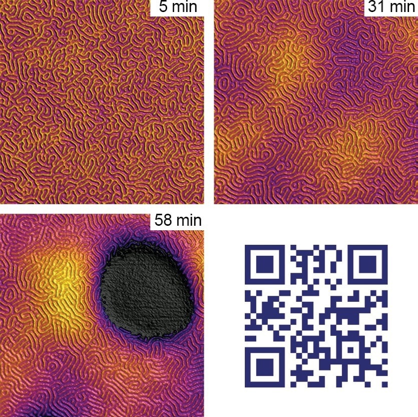
Figure 5. Solvent vapor annealing of a polystyrene-polybutadienepolystyrene (PS-PB-PS) triblock copolymer film. Films formed by spin casting organize into microphase morphologies that do not necessarily represent the lowest energy state. Annealing often results in restructuring, and solvent vapor techniques offer advantages over standard thermal annealing. Topography images were acquired continuously as the film was exposed to toluene vapor in a closed sample cell. Scan size 2 μm, line scan rate 10 Hz. Imaged with the Cypher ES. Image Credit: Asylum Research–An Oxford Instruments Company
AFM measurements performed in liquid or gas solvents frequently include specialized cells that encircle both the cantilever and sample. Cells can either offer a static environment or enable the perfusion of gases and liquids.
For a few film applications, corrosion and other electrochemical reactions are a significant consideration. Electrochemistry cells available for the AFM enable in-situ investigation of processes like film deposition or electroplating, corrosion, oxidation, and mass transfer.
With the availability of an electrochemistry cell, topographic imaging can accurately track nanoscale structural changes that are induced by electrochemical reactions (Figure 6).
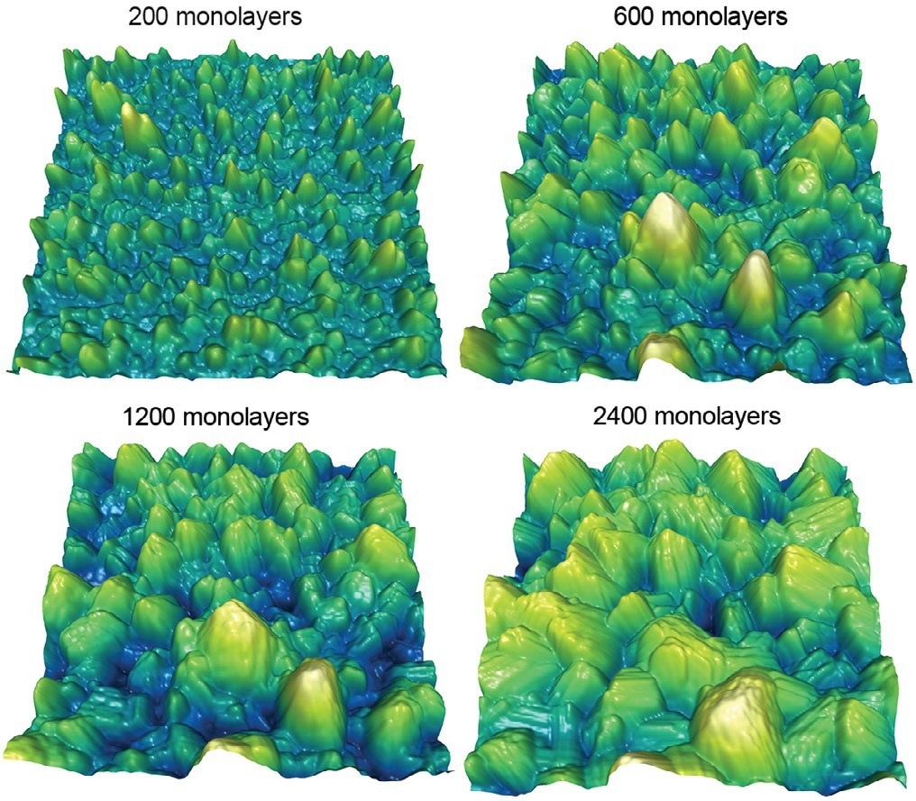
Figure 6. In-situ monitoring of zinc electrodeposition in an ionic liquid electrolyte. Zinc is an attractive material for electrodes in rechargeable batteries, but it can form detrimental morphologies that short circuit the cell. Uniform surface roughness that does not change with time reduces the probability of forming such features. These topography images show the morphology of a film grown at 325 mV deposition overpotential versus increasing film thickness (or equivalently, time). Surface roughness initially increased with thickness and time but eventually became constant (not shown). In contrast, the roughness always increased for films deposited at higher and lower overpotentials. Imaged with the MFP-3D AFM and the Electrochemistry Cell. Scan size 2 μm, height scale 200 nm. Image Credit: Adapted from Keist et al.8
Asylum AFMs for Solvent and Thermal Effects
- The Cypher ES AFM has a sealed cell that is compatible with even the harshest solvents and was created especially for precise environmental control. It allows for static or perfusion operation, as well as relative humidity control of gases. Precise temperature control is offered by the sample stages CoolerHeater (0 °C to 120 °C) and Heater (ambient to 250 °C).
- With the addition of temperature control provided by the BioHeaterTM (ambient to 80 °C), the Closed Fluid Cell for MFP-3D family AFMs enables static or perfusion operation in gas and liquid environments. For AFMs from the MFP-3D family, a humidity sensing cell is also available.
- With the PolyHeater (ambient to 300 °C), PolyHeater+ (ambient to 400 °C), and CoolerHeater (–30 to +120 °C) sample stages, temperature control is possible for MFP-3D AFMs.
- For strong electrochemical capabilities, the Electrochemistry Cell for MFP-3D family AFMs is made of chemically inert polyether ether ketone (PEEK).
Measuring Electrical, Electromechanical, and Magnetic Functionality
Several applications utilize the functional properties of a thin film — its magnetic, electric, or other response — to obtain the preferred performance. Instances include pyroelectric sensors, piezoelectric actuators, and ferroelectric nonvolatile memory. Topographic measurements on such films lend insight but do not directly evaluate functionality.
Hence, various AFM methods have been developed to quantify functional properties (Table 1).9–12 Such modes tend to leverage the exquisite force sensitivity of AFM to probe electrostatic, magnetic, and other interactions between the sample and the tip.
Table 1. AFM modes for functional properties. For each mode is shown its acronym as defined in the text, the physical quantity measured, and examples of information that can be acquired. Source: Asylum Research–An Oxford Instruments Company
| Mode |
What is sensed |
Information obtained |
| CAFM |
current |
conductivity, film uniformity and defects, dielectric breakdown, dopant distribution |
| EFM |
electrostatic forces |
electrostatic gradients, capacitance variations, embedded conductors |
| KPFM |
electric potential |
surface potential, work function, film uniformity and coverage |
| sMIM |
capacitance and resistance |
film thickness, dielectric constant, permittivity or conductivity variations, buried charge |
| PFM |
electromechanical response |
piezoelectric domains, polarization vector and switching, ferroelectric coercive field |
| MFM |
magnetostatic forces |
magnetic domains, magnetization hysteresis, magnetic coercive field |
The nanoscale spatial resolution of the AFM implies that measurements can be made on both patterned and uniform (blanket) films, for example for failure analysis of thin-film devices. Also, concurrent imaging of topography and functionality allows a deep understanding of local structure-property relations.
AFM modes to define electrical properties contain Kelvin Probe Force Microscopy, (KPFM), Conductive AFM (CAFM), and Electrostatic Force Microscopy (EFM).9 As observed in Figure 7, CAFM can easily detect conductivity changes at terrace steps in graphene. Also, electrical modes are useful for evaluating film uniformity and coverage.
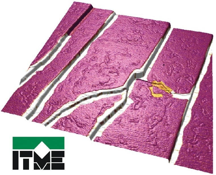
Figure 7. Electrical characterization of graphene with CAFM. The sample was a quasi-freestanding bilayer formed by chemical vapor deposition on a semi-insulating 4H-SiC (0001) (silicon carbide) substrate. The image shows CAFM current for a bias voltage of -1.5 V DC overlaid on topography. Areas with three regimes of electrical conductance can be identified: low (purple), intermediate (gold), and high (white). The step edges of the underlying substrate induce a resistance anisotropy that results in high conductance channels along the terrace steps. Scan size 10 μm, current scale 120 pA. Acquired with the Cypher S AFM and the ORCA™ CAFM module. Sample courtesy Institute of Electronic Materials Technology (ITME, Warsaw, Poland). Image Credit: Asylum Research–An Oxford Instruments Company
An associated method, Scanning Microwave Impedance Microscopy (sMIM),10 allows conductivity and permittivity measurements. Figure 8 displays the electrical permittivity imaging of buried structures.
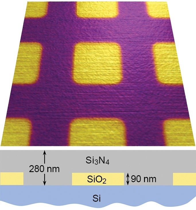
Figure 8. sMIM imaging of subsurface permittivity variations. The schematic diagram shows that the sample contained silica (SiO2 ) squares 90 nm thick buried under a thicker silicon nitride (Si3N4 ) film. After deposition of the Si3N4 film, the sample was polished so that topography variations were less than 0.5 nm. The image contains the relative capacitance signal obtained with sMIM overlaid on topography. The buried structures are clearly detected, despite little or no difference in topography. Scan size 20 μm. Acquired on the MFP-3D AFM. Image Credit: PrimeNano, Inc.
The characterization of piezoelectric, ferroelectric, and multiferroic films is made possible by the potent and adaptable capabilities of piezoresponse force microscopy (PFM).11 It offers nanoscale details on static and dynamic electromechanical responses, including domain structure, growth, and polarization reversal (Figure 2).
It can be difficult to get a decent signal-to-noise ratio when measuring thin films using traditional PFM methods without employing driving voltages that are too high to prevent polarization switching or even sample breakage and damage. Operating near the cantilever’s contact resonance frequency is one way to get more sensitivity at a lower driving voltage.
For nanoscale measurements of magnetic behavior to be performed, magnetic force microscopy (MFM)12 utilizes the interaction forces occurring between a magnetized tip and a magnetic sample.
It delicately probes functional properties of multiferroic and ferromagnetic films like those utilized in reading or write heads, high-density data storage, and spintronic devices.
MFM can offer data on magnetic vortices, magnetic domain patterns and walls, and even flux lines in superconductors. Similar to any other AFM method, MFM is considered an attractive characterization method since it offers high-resolution images and requires little or no sample preparation.
Also, it can be utilized in a range of environmental conditions. Figure 9 displays MFM studies to comprehend the impact of film deposition variables on magnetic domains.
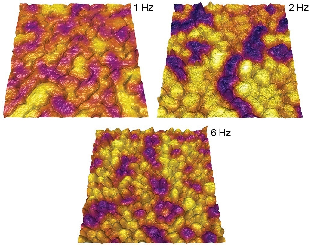
Figure 9. MFM evaluation of ferromagnetic FePt films grown by pulsed laser deposition (PLD). Understanding how magnetic behavior depends on PLD laser frequency could enable better control of film properties for applications such as data storage and recording. In these images, light (yellow) and dark (purple) regions represent domains polarized in the up and down directions, respectively. Overlaying the MFM phase signal on topography shows that the films deposited at 2 Hz and 6 Hz form single domain structures that correlate exactly with FePt islands. The 1 Hz film has a percolated morphology and forms multiple magnetic domains. Scan size 1 μm. Acquired with the MFP-3D AFM. Image Credit: Adapted from Golovchanskiy et al.13
Asylum AFMs for Electrical, Electromechanical, and Magnetic Functionality
- On AFMs from the Cypher and MFP-3D families, the ORCA module offers exceptional CAFM capabilities. For sensitive measurements over a wide current range (~1 pA–20 nA), it has an exclusive low-noise amplifier. An even wider current range (~1 pA–10 μA) is possible with the Dual Gain ORCA option.
- In comparison to conventional probe stations, NanoTDDB is an exclusive Asylum mode that can measure time-dependent dielectric breakdown on length scales as small as ~20 nm. In NanoTDDB, which is based on CAFM, a tip-sample voltage is applied up until a breakdown event is found. The voltage can be maintained constant or increased by ±220 V or ±150 V (system dependent).
- Asylum provides the only commercial high-voltage PFM mode (up to ±220 V or ±150 V depending on the system). All Asylum AFMs come equipped with software that fully integrates resonance-enhanced PFM for high sensitivity using either the patented Dual ACTM Resonance Tracking (DART) technique or the premium Band Excitation option.
- sMIM is a mode for scanning microwave impedance microscopy that is integrated exclusively with MFP-3D family and Cypher S AFMs. Electrical permittivity and resistivity variations on insulators, semiconductors, and conductors can be imaged thanks to this technique.
- For all MFP-3D family AFMs except Origin, the Variable Field Module 3 provides additional flexibility for studies of magnetic field dependence. It can produce adjustable fields up to ±0.75 T in plane. The innovative permanent magnet design prevents heating and the resulting drift.
Measuring Mechanical Properties
As far as other applications are concerned, mechanical properties like hardness, modulus, and friction are crucial to the function of the film. For instance, wear-resistant films enhance performance in products ranging from razor blades to hip replacements.
Mechanical properties are also significant when it comes to obtaining total product reliability and durability. For example, fracture toughness and low modulus in low-k dielectric films could result in fracture and delamination at the time of combination with copper interlinks.
With the help of its high force sensitivity and spatial resolution, the AFM has strong abilities for quantifying nanoscale mechanical properties. It is possible for AFM-based methods to be applied at much lower forces than traditional nanoindentation, thereby leading to smaller indentation depths.
This allows much thinner films to be probed in the absence of artifacts as a result of the substrate. The high lateral spatial resolution of the AFM implies that heterogeneous and patterned films can be assessed in a direct manner. Force curves are a renowned technique for quantifying elastic modulus.14
But several film materials are comparatively rigid (modulus >10 GPa), and so it could be hard or impossible to produce high enough forces along with standard cantilevers to adequately indent them. Also, traditional force curve mapping is very slow, even though the recent initiation of Fast Force Mapping enables much quicker operation.
Two AFM modes that were developed recently, AM-FM Viscoelastic Mapping Mode and Contact Resonance Viscoelastic Mapping Mode, provide both greater speed and quantitative nanomechanical measurements on higher-modulus materials. Such modes could be utilized for both quick, qualitative contrast imaging as well as highly advanced quantitative mapping (Figure 10).
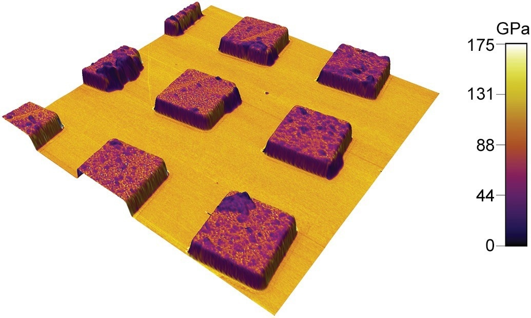
Figure 10. Elastic modulus image of a patterned titanium film on silicon, overlaid on topography. blueDrive photothermal excitation on the Cypher AFM was used for DART contact resonance imaging. Note the strong contrast between these two very high modulus materials. Scan size 25 μm. Image Credit: Asylum Research–An Oxford Instruments Company
Specifying nanoscale tribology15 is considered paramount for several film applications. Force curves could be utilized to quantify surface adhesion, while methods like lateral force microscopy (LFM) yield data on frictional forces.
LFM includes moving the tip sideways while being in contact with the sample and quantifying the cantilever deflection in the horizontal photodiode channel. LFM could be utilized to image spatial changes in the lateral force or to obtain friction loops of the lateral force versus sliding distance (Figure 11). Calibrated measurements at various applied loads can be utilized to identify the coefficient of friction.
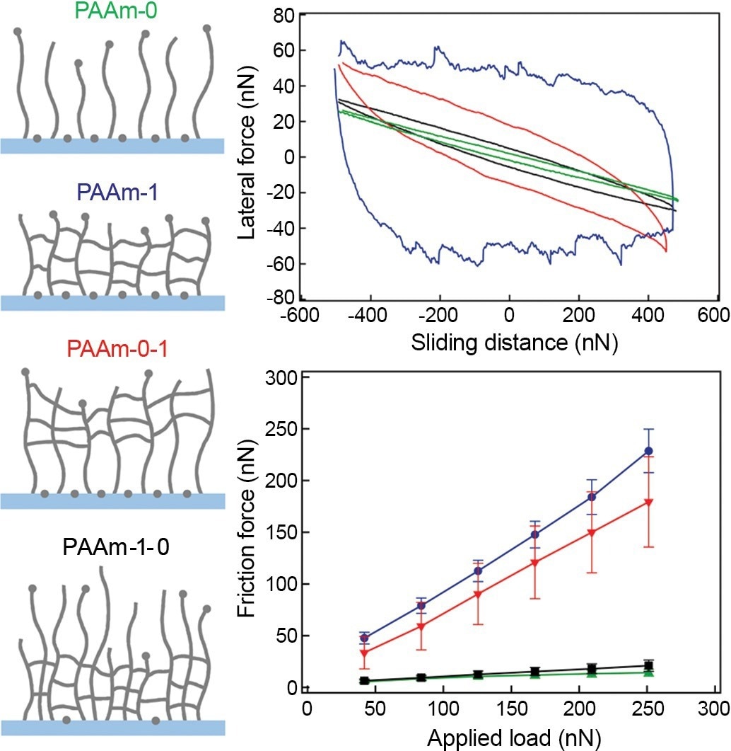
Figure 11. Nanotribology of layered polymer brush-gel films. Mechanically-graded layers with both high modulus and toughness occur frequently in nature, but synthesis of an all-polymer counterpart remains challenging. As shown in the simplified schematics, two layer films of polyacrylamide (PAAm) on silicon were created with either a brush supporting a crosslinked brush-hydrogel (“gel”) or a gel supporting a brush. LFM experiments were performed in water with different film configurations: pure brush (PAAm-0), pure gel (PAAm-1), brush-gel (PAAm-0-1), and gel-brush (PAAm-1-0). The top graph shows friction loops of lateral force versus sliding distance and the bottom, friction force versus applied load. (Curves are color-coded to film type.) The films displayed different tribological behavior, but the response was always determined primarily by the structure of the film’s outer layer where the sliding occurred. Acquired on the MFP-3D AFM with the Closed Fluid Cell. Image Credit: Adapted from Li, et al.16
Asylum AFMs for Nanomechanical Properties
Users can choose the method that is best for a given application from the many techniques that Asylum provides for nanomechanical measurements.
On films thicker than a few hundred nanometers, the MFP-3D NanoIndenterTM option enables measurements of elastic modulus and hardness that are truly ISO-compliant.
The MFP-3D Infinity and Cypher AFMs’ Fast Force Mapping Mode makes force curve mapping less frustrating by acquiring complete images in minutes rather than hours (<10 minutes for 256 × 256 pixels).
Utilizing well-known tapping-mode principles, Asylum's unique AM-FM Viscoelastic Mapping Mode enables high-speed mapping of elastic modulus E' and viscoelastic loss tangent. Favorable for 100 kPa < E’ < 100+ GPa.
Contact Resonance Viscoelastic Mapping Mode offers additional capabilities for quantitative mapping of elastic storage modulus and viscous loss modulus on all Asylum AFMs. Best for 1 GPa < E’ < 100+ GPa.
Get Results with Asylum AFMs
This article only scratches the surface of the potential of AFMs for characterizing thin films and coatings. AFMs can map nanoscale functioning in a remarkable number of ways and assess 3D surface roughness with extraordinary spatial precision.
High spatial resolution and sensitivity are only two of the amazing technological advantages that Asylum AFMs possess. They also contain features that increase productivity and user-friendliness, such as quick scanning and automated processes. Contact Asylum Research to learn more about how AFMs may improve the job.
References
- M. Ohring, Materials Science of Thin Films: Deposition and Structure, 2nd ed. (Academic Press, San Diego, CA, 2002).
- T. Mehmood, A. Kaynak, X.J. Dai, A. Kouzani, K. Magniez, D.R. de Celis, C.J. Hurren, and J. du Plessis, Mater. Chem. Phys. 143, 668 (2014).
- A. Duk, M. Schmidbauer, and J. Schwarzkopf, Appl. Phys. Lett. 102, 091903 (2013).
- B. Bhushan, “Surface Roughness Analysis and Measurement Techniques,” in Modern Tribology Handbook Vol. 1 (CRC Press, Boca Raton, USA, 2001), Chap. 2.
- M. Gu, S.A. Wolf, and J. Lu, Adv. Mater. Interfaces 1, 1300126 (2014).
- A.R. Damodaran, S. Lee, K. Jambunathan, S. Maclaren, and L.W. Martin, Phys. Rev. B 85, 024113 (2012).
- E.S. Gadelmawla, M.M. Koura, T.M.A. Maksoud, I.M. Elewa, and H.H. Soliman, J. Mater. Process. Technol. 123, 133 (2002).
- J.S. Keist, C.A. Orme, P.K. Wright, and J.W. Evans, Electrochim. Acta 152, 116 (2015).
- R. Berger, H.-J. Butt, M.B. Retschke, and S.A.L. Weber, Macromol. Rapid Commun. 30, 1167 (2009).
- K. Lai, W. Kundhikanjana, M.A. Kelly, and Z.X. Shen, Appl. Nanosci. 1, 13 (2011).
- S.V. Kalinin, B.J. Rodriguez, S. Jesse, E. Karapetian, B. Mirman, E.A. Eliseev, and A.N. Morozovska, Annu. Rev. Mater. Res. 37, 189 (2007).
- U. Hartmann, Annu. Rev. Mater. Res. 29, 53 (1999).
- I.A. Golovchanskiy, A.V. Pan, S.A. Fedoseev, and M. Higgins, Appl. Surf. Sci. 311, 549 (2014).
- H.J. Butt, B. Cappella, and M. Kappl, Surf. Sci. Rep. 59, 1 (2005).
- R.W. Carpick and M. Salmeron, Chem. Rev. 97, 1163 (1997).
- A. Li, S.N. Ramakrishna, P.C. Nalam, E.M. Benetti, and N.D. Spencer, Adv. Mater. Interfaces 1, 1300007 (2014).

This information has been sourced, reviewed and adapted from materials provided by Asylum Research - An Oxford Instruments Company.
For more information on this source, please visit Asylum Research - An Oxford Instruments Company.