Sponsored by Nanosurf AGReviewed by Olivia FrostJan 10 2023
The word “piezo” derives from the Greek word piezein, meaning “to press tightly”. Piezoelectricity refers to a material’s ability to convert mechanical energy (pressing) into electric energy (polarization) and vice versa. The direct piezoelectric effect produces electric polarization in response to applied stress.
Directionality and magnitude of polarization are proportional to the applied stress, and the polarization is usually comprised of components in parallel and perpendicular directions. The reverse phenomenon, the inverse piezoelectric effect, is a mechanical deformation in response to the application of an electrical field. Piezoelectric materials are widespread and can be found in common use in our everyday lives.
For instance, ferroelectric materials are a subset of piezoelectric material that have an intrinsic spontaneous polarization and are used in capacitors, ultrasound imaging, non-volatile memory, data storage, light deflectors, thermistors, filters, oscillators, modulators, and monitors, amongst others. Atomic force microscopes (AFM) depend on the inverse piezoelectric effect in their scanner design and functionality.
With the miniaturization of components being a continuous factor across the electronics industry, piezoelectric thin films have also become a key area of interest (e.g. functionally coated flexible glass). Thin films demonstrate piezoelectric behavior in specific regions (often called domains) in the subnanometer regime. Knowing the domain size and their response under an applied electric field allows for dynamic measurements of domain switching and local hysteretic behavior.
These material properties mean that researchers can understand structure-function relationships for material design. AFM can measure the local inverse piezoelectric response with high fidelity and offer high-resolution piezoelectric information with parallel surface topography. This mode of operation of AFM is typically known as Piezo Response Force Microscopy (PFM). PFM helps measure deformations in the subnanometer regime and map ferroelectric domains with a lateral resolution of just a few nanometers.
How Does it Work?
AFM is a method of surface characterization that rasters a fine needle at the free end of a cantilever across the surface of a sample. Light bounces off the back of the cantilever onto a position-sensitive photodiode that detects the motion of the cantilever.
In PFM mode, AFM functions in contact mode, where the cantilever constantly interacts with the sample at a consistent force. To apply an electrical field across the sample, a sample is placed onto a conductive substrate, and a conductive cantilever is applied as the second electrode.
Either electrode can be selected to apply the voltage, though the first tends to perform better. The schematics of a PFM setup are displayed in Figure 1. To determine the piezo response, applying an AC voltage between the tip and the substrate caused a periodic expansion and contraction of the sample.
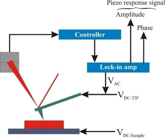
Figure 1. Schematic of a Piezo-response Force Microscopy experiment. Voltage is applied to a conductive tip in contact with sample and mechanical deformation of the sample is measured by the deflection of the laser. Image Credit: Nanosurf AG
With constant contact between the tip and the sample, the oscillatory movement of the sample surface causes a periodic cantilever bending that the AFM controller’s lock-in amplifier uses to conduct the analysis.
The amplitude and phase response of the cantilever are recorded during PFM imaging. Phase contrast in PFM offers information relative to the direction of the electrical polarization in correlation with the electrical field. The amplitude demonstrates the magnitude of the piezo response and can usually be used to identify features such as the domain wall positions.
The electrical polarization can have components both parallel/antiparallel and perpendicular to the applied field. Vertical and lateral bending of the cantilever are also observed due to the AC field instigating in out-of-plane and in-plane oscillations of the sample surface as denoted in Figure 2.
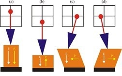
Figure 2. Schematics of (a-b) vertical and (c-d) lateral PFM mode. The applied electric field (E) and polarization (P) directions are denoted with arrows. Vector PFM is performed by combining data with a 0° and 90° rotation of the sample to obtain 3D vector information of the response. Image Credit: Nanosurf AG
If the observed response is completely parallel/antiparallel to the field (Figure 2a,b), the out-of-plane amplitude and phase of the vertical cantilever bending supplies direct information relative to the magnitude and polarization (parallel vs. anti-parallel) of the sample deformation.
If the polarization and electric field are perpendicular to one another (Figure 2c,d), the result will be in-plane movement of the sample. With a purely out-of-plane response, the effective piezoelectric coefficient, d33, can be determined from the measured amplitude (A) of the oscillation and the voltage applied across the sample (VAC):
d33 = A/VAC
Below the cantilever's resonance frequency, amplitude A can be expressed in pm (by converting voltage to distance using the cantilever deflection sensitivity), and the piezoelectric coefficient can be quantitatively measured. However, it is not so simple to compare d33 measurements acquired using AFM with other bulk techniques. It is widely regarded that material properties can vary considerably on the nanoscale compared to the bulk, and the piezoelectric effect is not exempt. In practice, materials can present a mechanical response in three dimensions.
Movement in-plane and out-of-plane in relation to the sample surface may occur in response to the voltage applied. To capture this, vector PFM is utilized to monitor both the vertical and lateral deflection of the cantilever. Moreover, a sample area is measured at two rotational orientations in relation to the cantilever.
Mathematical reconstruction of data facilitates combining both the in-plane and out-of-plane vector components to create a 3D map of the piezo response. AFM has applications beyond imaging as a means of spectroscopy, locally induced polarization at the tip to understand material hysteresis, or writing domains using lithography.
Experimental Setup
As displayed in Figure 1, PFM necessitates the use of an AFM that can capture electrical measurements with conductive cantilevers. To determine both the out-of-plane and in-plane responses, two independent internal lock-in amplifiers are necessary to measure the amplitude and phase of each component.
A camera view that facilitates overhead viewing of the sample to determine areas of interest is a key factor, as shown in Figure 3. This is particularly useful for 2D materials as the flakes of interest must be directly located and positioned under the cantilever.
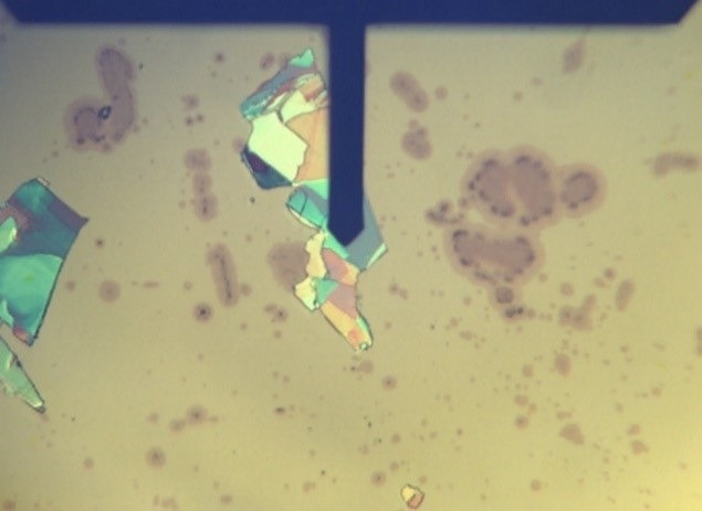
Figure 3. A top view camera image is essential for most PFM samples. This image shows flakes of 2D material on a gold substrate. Flakes of different thickness appear as different colors in the image. Image Credit: Nanosurf AG
Numerous practical aspects of PFM are crucial, including sample preparation and cantilever choice. While flat samples are typically suitable when conducting PFM in its basic state, some rougher samples, including ceramics, may require polishing before imaging techniques.
Care should be taken to ensure working with contamination-free surfaces. A thick insulating layer between the conductive substrate and sample should be avoided, as this will limit the field strength across the sample and the piezo response.
Conductive cantilevers for PFM have an extensive range of force constants that vary from 40 N/m with a resonance frequency range between 10-400 kHz. Stiffer cantilevers reduce the contribution of electrostatic interaction with samples, whereas softer probes limit tip wear and are less prone to sample damage during scanning.
While Pt/Ir coated probes can be utilized for conducting PFM measurements, studies have revealed that conductive diamond or PtSi-coated tips demonstrate enhanced stability of the PFM signal. Another critical measurement parameter is the optical sensitivity, which is inversely proportional to the probe length.
Therefore, shorter cantilevers transmit better signals. Specialized PFM measurements such as high-voltage PFM (HV-PFM) and dual frequency response tracking (DFRT) necessitate additional instrumentation. For HV-PFM, an additional high-voltage amplifier is networked to a user output of the AFM controller and controlled directly from the AFM software.
Calibration of the user channel is carried out so that the user can set the output voltage of the HV amplifier directly. For this mode, Nanosurf equipment can be paired with an external lock-in amplifier from Zurich Instruments, and signals can be transmitted via user input channels.
Zurich Instruments' lock-in amplifiers are robust tools, not only suitable for PFM applications, but other state-of-the-art AFM modes, including frequency modulated, heterodyne Kelvin Probe Force Microscopy (KPFM), and other multi-frequency applications.
Traditional PFM Applications
Lithium niobate (LiNbO3) is a dynamic ferroelectric material used extensively in applications ranging from waveguides to piezoelectric sensors. A PFM measurement is exhibited in Figure 4. This sample is periodically poled and demonstrates a pure out-of-plane response with fluctuating domains parallel and antiparallel to the applied field.
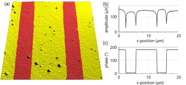
Figure 4. Vertical PFM images of periodically poled lithium niobate. (a) Representative topography with phase information color overlaid for a 20x20 μm2 area showing, (b) horizontal profile of the amplitude and (c) phase, showing little influence of amplitude with polarity and the 180° phase shift as expected. Data courtesy: Brian Odermatt, EPFL/Nanosurf. Image Credit: Nanosurf AG
At ambient conditions, the piezo response remains stable over a vast voltage range of the electric field applied. The polarization does not influence the piezo response's topography and magnitude (amplitude signal), but phase changes by 180° signal that the electrical polarization is moving towards the out-of-plane direction. The amplitude demonstrates no significant changes between the oppositely poled domains.
Ferroelectric 2D materials and thin films have garnered interest as they show application potential in energy, electronics and optoelectronics industries.
PFM of CuInP2S6 flakes on a silicon substrate is displayed in Figure 5. The PFM measurement offers the magnitude of the vertical deformation (amplitude image, Figure 5a) and the corresponding polarization direction (phase image, Figure 5b).
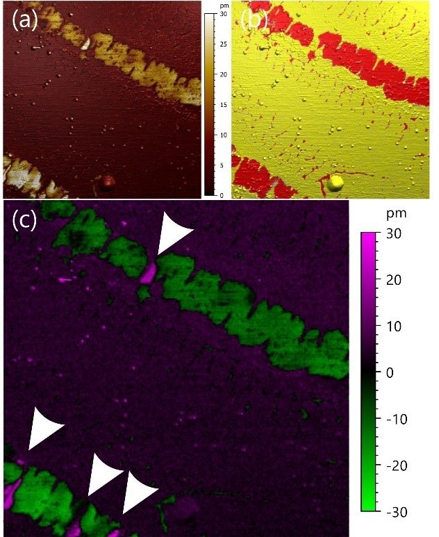
Figure 5. Vertical PFM imaging of 2D ferroelectric CuInP2S6 on Silicon substrate. (a) amplitude (b) phase and (c) amplitude projection, all represented as a color overlay on the topography. Image size: 5x5 μm2 (color scales do not include illumination effects from the topography visualization). Image Credit: Nanosurf AG
To distinguish the polarization direction of amplitude more easily, the amplitude and phase information can be paired using an amplitude projection (Figure 5c). By multiplying the amplitude by the cosine of the phase, which is 0° or 180°, the sign remains consistent with the polarization direction, and distinct domains can be observed more easily (Figure 5c, arrow heads).
Ferroelectric thin films can be characterized in a relatively straightforward manner using PFM. Figure 6 reveals the piezoelectric characterization of a piezoelectric and high-magnetostrictive thin film cultivated using a sol-gel process on a flexible glass substrate. The surface topography exhibits "protrusions" with a dome-like morphology that are microns across (Figure 6a).
The amplitude projections of the out-of-plane response (Figure 6b) and the in-plane response (Figure 6c) highlight the differences in domain size and structure within individual dome-like protrusions on the sample.
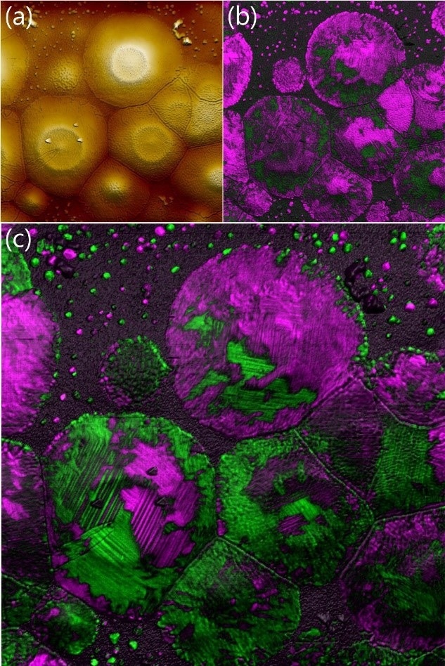
Figure 6. Out-of-plane and in-plane PFM response recorded on a 800 nm PZT thin film, grown by sol-gel method on Pt(111)/Ti/Flexible glass. (a) Topography, (b) out-of-plane amplitude projection, (c) in-plane amplitude projection. Image size: 9x9 μm2 (color scales do not include illumination effects from the topography visualization). Data courtesy: Dr. Itamar Neckel, Brazilian Center for Research in Energy and Materials – CNPEM, Brazilian Synchrotron Light Laboratory LNLS. Image Credit: Nanosurf AG
Dual Frequency Resonance Tracking (DFRT) PFM
When taking conventional PFM measurements, the probe oscillates at frequencies far below the cantilever's resonance frequency ( Figure 7a). A primary advantage of working at these frequencies is that the deflection can be easily converted into picometers, leveraging the deflection sensitivity of the cantilever.
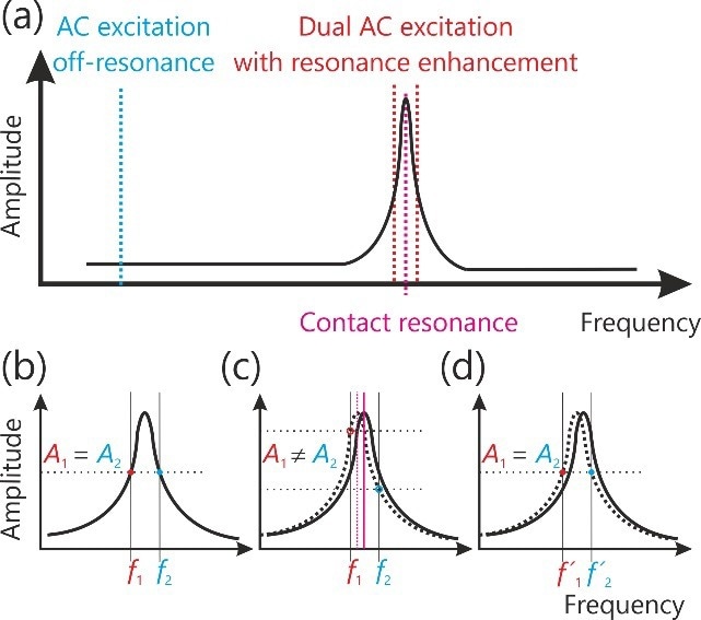
Figure 7. Schematics showing (a) traditional PFM measurement in off resonance mode and dual frequency resonance enhanced PFM mode. (b-d) DFRT amplitude response upon a change in contact resonance frequency. Image Credit: Nanosurf AG
However, signals tend to be small and require complex measuring procedures, particularly for thin samples.
The piezo response can be improved by working at a resonance frequency of the cantilever. Since PFM is usually conducted in contact mode, the resonance frequency first observed is the contact resonance, where the cantilever makes a buckling movement between the tip and the base of the fixed cantilever.
The sample is applied as a “shaker piezo”, to oscillate the cantilever in its (contact) resonance, which is about 4-5 times more than the basic resonance frequency of the cantilever that remains fixed at one side.
Working at the contact resonance is vulnerable to crosstalk between the PFM response and other tip-sample interactions because the contact resonance is dependent on the local stiffness of the sample. To prevent any crosstalk, the DFRT mode was applied.
When introducing the DFRT mode, an AC voltage is applied at two frequencies on both sides of the contact resonance peak with equal amplitude (Figure 7b). When there is a shift in contact resonance, the amplitudes also experience a shift (Figure 7c). A feedback algorithm in the lock-in amplifier offsets the difference by modulation of the excitation frequencies.
The difference Δf between the two excitation frequencies remains fixed in feedback (Figure 7d). The application of this method allows for changes in the contact resonance frequency to be decoupled from the PFM response. Contact frequency enhanced PFM can be applied to study the piezo-ceramic material, lead zirconate titanate (PZT).
Moreover, fashioning a remedy for fatigue and retention of PZT can be made by adding small amounts of donor dopant, such as the ions of La3+. PFM can then examine grain and domain morphology with signal improvement at the contact resonance frequency, as illustrated in Figure 8. As a demonstration of DFRT, the PFM phase signal of a thin film of CuInP2S6 is displayed in Figure 9.
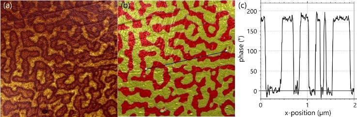
Figure 8. PFM measurement at contact resonance frequency (a) amplitude (arbitrary units), (b) phase (c) profile In the phase, showing domain widths ~100 nm range. Excitation: VAC=5 V at f=304 kHz, Cantilever: Pt-coated Si with nominal spring constant k=1.5 N/m. Image size: 3x3 μm2. Sample courtesy: Prof. A. Kholkin, University of Aveiro, Portugal, data courtesy: Sergei Magonov, SPM labs, AZ. Image Credit: Nanosurf AG
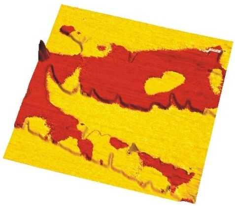
Figure 9. Piezo phase response from a thin film CuInP2S6 grown on a silicon surface imaged with DFRT PFM showing oppositely polarized domains while applying <1 V of AC modulation. Image Credit: Nanosurf AG
Regardless of the modulation amplitude being less than 1V, the amplification by the contact resonance delivers enhanced contrast and reveals clear borders between oppositely polarized domains for visualization. When applying DFRT, quantification of the amplitude of the response can be much more complicated than when performing conventional PFM.
The conversion of the amplitude to picometers necessitates extra calibration steps, as it depends on the quality factor of the contact resonance and the deflection sensitivity relative to the buckling movement.
Spectroscopy and High-voltage PFM
To go beyond imaging, AFM can also be applied for spectroscopy and to "write" domains locally by introducing a DC bias to the sample. In spectroscopy, the amplitude and phase of the piezo response are determined as a function of a bias voltage applied over the sample. One of the primary applications of spectroscopy is to identify the required voltage for domain reversal.
In ferroelectric materials, the external voltage needed to reverse a polarization is known as the coercive field. To achieve the coercive field, bias voltages exceeding ±10 V may be required. A high-voltage amplifier is paired with a user output, and voltages up to ±200 V can be applied.
AC voltages can also be introduced using the high-voltage (HV) amplifier to boost the signal-to-noise ratio of weak piezoelectric properties.
To conduct HV-PFM, the sample must be stable when exposed to high voltages and safeguard the user against any physical harm or prevent damage to electronic equipment. Necessary care is required to ensure no electronics are exposed when high voltages are applied.
However, increasing bias voltage offset enhances the contribution of electrostatic forces on the cantilever. This electrostatic contribution may even surpass the PFM response, concealing domain reversal.
To reduce the effect of electrostatics, switching spectroscopy PFM (SS-PFM) is a suitable method. Rather than increasing the voltage linearly, a train of voltage pulses is applied, cutting off the voltage difference in between.
As switching occurs, the AC voltage is applied continuously to record the PFM response both in the on and off states of the voltage. This is depicted schematically in Figure 10. The “on” and “off” states determine the status of the DC bias voltage.
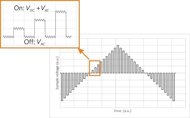
Figure 10. Schematic diagram of SS-PFM measurement depicting a train of DC bias pulses on top of an AC modulation. Image Credit: Nanosurf AG
While the DC voltage is applied to alter the polarization, the AC voltage is utilized to measure the piezoelectric signal simultaneously. To demonstrate SS-PFM, the amplitude and phase behavior of a P(VDF-TrFE) thin film is displayed in Figure 11.
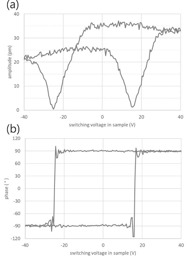
Figure 11. Piezo response hysteresis loop of P(VDF-TrFE) thin film (a) amplitude vs applied voltage and (b) phase vs applied volt-age obtained by SS-PFM. Sample courtesy: Joanneum Research Forschungsgesellschaft mbH, Austria. Image Credit: Nanosurf AG
The data were recorded during the off phase of an SS-PFM experiment. An HV amplifier applied pulses between -40 V and +40 V. As the voltage pulses were incrementally increased, the polarization switching was observed at +16 V. This is represented by the amplitude dropping to zero and the 180° phase shift. As the voltage was turned down, the polarization returned to -25 V, switching back to the starting point.
Polarization and Lithography
Once the voltage needed to overcome the coercive field is revealed, for instance, from an SSPFM experiment, the tip can be applied to polarize the sample locally. Lithography can write single domains, domain arrays, and complex patterns without altering the surface topography. PFM high-voltage lithography on a P(VDFTrFE) thin film is shown in Figure 12.
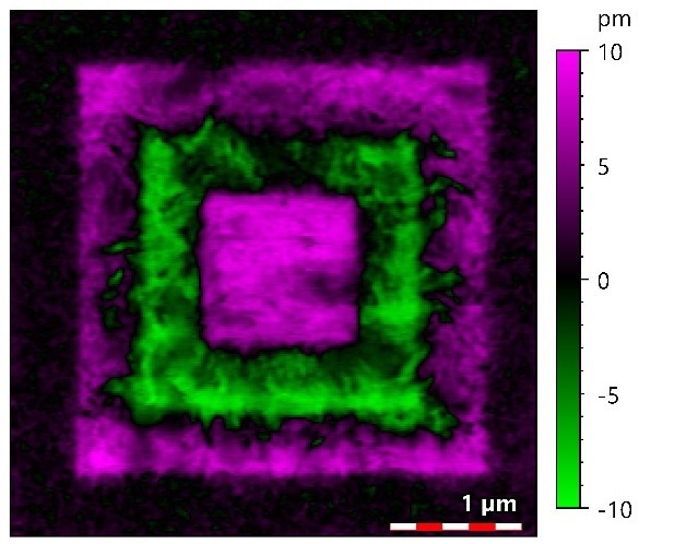
Figure 12. PFM amplitude projection of P(VDF-TrFE) thin film after applying DC sample bias of 40 V, -40 V, and 40 V during consecutive scanning of 3x3 μm2, 2x2 μm2, and 1x1 μm2 areas, respectively. The AC amplitude amounted to 5 V. Sample courtesy: Joanneum Research Forschungsgesellschaft mbH, Austria. Image Credit: Nanosurf AG
The tip was biased and scanned in square regions to polarize regions intentionally and switch the direction of the polarity of a smaller region. First, imaging of a 3x3 μm2 area was performed while a bias voltage of +40 V was applied to the sample substrate.
Subsequently, the polarization was reversed by scanning areas of 2x2 μm2, and 1x1 μm2 respectfully and applying -40 V and +40 V accordingly.
Figure 12 demonstrates a 4x4 μm2 image of the PFM amplitude projection (amplitude multiplied with the cosine of the phase) on the P(VDF-TrFE) film once manipulation steps had been performed.
Beyond the most significant area, there is no polarization of the thin film, and the amplitude is consequently small. After polarization with a positive substrate voltage, the sample indicates zero phase and high amplitude, marked by the magenta color. The 500 nm green region exhibits polarization reversal, with similar amplitude, but due to the 180° phase difference, it shows the opposite sign.
The magenta inner square depicts a 1x1 μm2 region, where the polarization reversal occurred for a second time. Interestingly, the domain borders between the oppositely polarized regions extend into the adjacent regions, suggesting collective switching of domains beyond the tip-sample contact area.
Conclusion
Understanding material piezo-responsive behavior will continue to be an essential study area for advancing many technologies. Characterization on the nanometer scale is now possible and necessary as the miniaturization of electronics continues to pick up pace.
PFM allows researchers to study the electromechanical properties of materials with nanometer spatial resolution and picometers of sensitivity in innovative ways. Nanosurf PFM capabilities extend beyond conventional PFM imaging to enhance signal-to-noise, perform lithography, measure switching dynamics, and apply high voltages relative to the experiment needs.
Notes:
- PFM is available on CoreAFM, FlexAFM and DriveAFM from Nanosurf.
- AFM and PFM images were processed with MountainsSPIP 9.

This information has been sourced, reviewed and adapted from materials provided by Nanosurf AG.
For more information on this source, please visit Nanosurf AG.