Nanosurf, using its experience in industrial metrology systems, created the Alphacen 200 Drive, a sophisticated AFM system designed to satisfy the semiconductor industry's exacting requirements.
The Alphacen 200 Drive addresses the difficulties commonly encountered by semiconductor manufacturing and research, from challenging electrical characterization tasks with SMM to unmatched low-noise roughness analysis with WaveMode.
Features
Performance
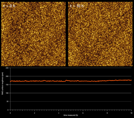
Time-series of surface roughness measurements of a silicon wafer using WaveMode. Images in the top row show images at the beginning of the series and after 10 h. The graph below shows the roughness determined from each image of the series. Image Credit: Nanosurf AG
The Alphacen 200 Drive is carefully designed to satisfy the complex requirements of semiconductor research and development. Because of its unique flexure tip scanner architecture, this cutting-edge atomic force microscope is excellent at taking pictures at the atomic level.
The CleanDrive photothermal excitation approach ensures reliable and low-noise operation, enabling comprehensive investigation of surfaces with low roughness. Furthermore, the Alphacen 200 Drive includes WaveMode, the quickest off-resonance imaging mode available, allowing it to gently capture even the smallest structures.
Versatility
Image Credit: Nanosurf AG
The features of the Alphacen 200 Drive AFM system go beyond high-resolution imaging and remarkable stability. The broad scan range of 100 × 100 × 20 μm3 enables full investigation of huge samples, highlighting its versatility. This versatility extends to compatibility with a wide range of nanoelectrical characterization methods (NEC), including Nanosurf’s Scanning Microwave Microscopy (SMM) solution.
Researchers can further customize the Alphacen 200 Drive's capability with a variety of accessories and software options, ensuring that the system remains responsive to their individual research requirements in semiconductor research and development.
Automation

Image Credit: Nanosurf AG
Explore how completely automated laser alignment and cantilever calibration might improve the measuring procedure. To achieve precise and consistent roughness and dimensions measurements across the whole range, employ the Alphacen 200 Drive's WaveMode and programmable, completely addressable 200 × 200 mm2 sample stage.
Obtaining the Highest Resolution with a Large Scanner
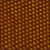
Atomic lattice of gypsum. Image Credit: Nanosurf AG
Thanks to the superior technology of the DriveAFM scan head, imaging at atomic resolution is now achievable on this large-stage system.
This powerful combination makes a wide range of structures accessible for analysis by enabling the observation of feature sizes spanning multiple orders of magnitude.
Gain Insight into the Local Nanoelectrical Properties
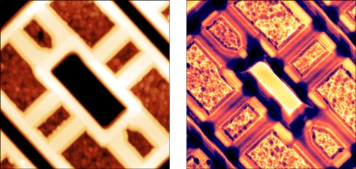
Topography (left) and imaginary part of the complex S11 parameter representing local capacitance (right). Image Credit: Nanosurf AG
The Alphacen 200 Drive, when combined with Nanosurf's SMM solution, allows for exact electrical characterization at the nanoscale. Researchers can measure the local capacitance, carrier density, resistance, conductivity, and dielectric constant of structures in cutting-edge integrated circuits.
SMM can also assess subsurface elements in complex multilayered architectures. This innovative SMM solution ensures the shortest time to results, allowing for a more thorough understanding of materials in semiconductor research and development.
Alphacen 200 Drive Features
- Linear and Flat Scanning
- Numerous AFM Modes
- Automatic Cantilever Alignment
- Scan Range of 100 μm
- 28-bit CX Controller
- WaveMode
- Sample Observation Camera
- Simple to Use
Imaging Modes
Alphacen 200 Drive Operating Modes
Standard Imaging Modes
- Static Force Mode
- Lateral Force Mode
- Dynamic Force Mode (Tapping Mode)
- Phase Imaging Mode
Electrical Properties
- Conductive AFM (C-AFM)
- Scanning Spreading Resistance Microscopy (SSRM)
- Piezoelectric Force Microscopy (PFM)
- Electrostatic Force Microscopy (EFM)
- Kelvin Probe Force Microscopy (KPFM)
- Magnetic Force Microscopy (MFM)
- Scanning Microwave Microscopy (SMM)
Advanced Imaging Modes
- WaveMode
- CleanDrive photothermal excitation
Mechanical Properties
- Force Spectroscopy (Unfolding and Stretching, Adhesion)
- Force Modulation
- Force Mapping (Stiffness and Modulus, Adhesion)
Lithography and Nanomanipulation
Electrochemical AFM (EC-AFM)
Scanning Thermal Microscopy (SThM)
Nanosurf Studio
After carefully examining the real user experience of doing atomic force microscope measurements, the application scientists and software engineers returned to the drawing board to develop a user interface that lets users concentrate on the measurement and its outcomes. Anticipate a fresh release with enhanced features every quarter. Simply hit the play button.
- Configure each software GUI for both experienced and inexperienced users
- Automated AFM configuration (data collection, approach, spring constant and sensitivity calibration, laser alignments)
- ViewPort optical sample navigation
- Quarterly updates that include bug fixes, enhanced workflows, and new features
- Novice users can easily learn, and experienced users have complete flexibility
- Instrument control is fully scriptable