Sponsored by Nanosurf AGReviewed by Olivia FrostNov 2 2023
Nanosurf is a leading provider of innovative atomic force microscope (AFM) measurement equipment. By delivering measurement solutions for quality control, Nanosurf contributes to the progression of the semiconductor industry.
This article discusses delivering advanced, cleanroom-compliant, automated AFM solutions for the semiconductor industry – focusing specifically on the following key areas.
Design Challenges and Solutions
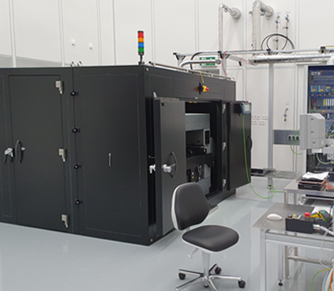
Nanosurf’s AFM machines house large, non-planar samples (that are hundreds of millimeters in diameter) while still permitting complete sample coverage.
AFM systems have historically only been able to accommodate small samples that are a few millimeters or centimeters in diameter. The main reason for this is that for a small mechanical loop, i.e., the shortest track through the AFM hardware that mechanically connects the AFM cantilever tip and the actual measurement site, it is easier to achieve good system stability and, thus, low noise levels.

Image Credit: Nanosurf AG
Opposed to standard AFM systems, a large mechanical loop is fundamental to systems that host large samples. The main challenge of designing and constructing such systems is attaining the appropriate noise level (RMS) on the PM scale.
Nanosurf uses finite element method (FEM) simulations to determine the performance of the system, taking into account mechanical stresses. When operating at the physical limits, these calculations require close collaboration with suppliers to model their components accurately during the design phase.
Satisfying the challenging performance standards and strict safety demands causes an interplay between mechanical and control design. Thus, machine control and software are developed alongside the mechanical design procedure.
Numerous rounds of system design evaluations, plus subsequent improvements and safety evaluations (with modifications of sensors and safe communication pathways), are conducted to attain the necessary performance standards. During the commissioning phase, user-machine interaction must also be considered.
Automation and Process-Oriented Operation
Nanosurf’s industrial AFM measurement systems enable automation of the entire sample analysis process, from sample handling to specimen-specific measurement procedures. This additionally involves automated cantilever exchange and specimen re-positioning with sub-micron re-positioning accuracy.
A real-time programmable logic control (PLC) is essential for ensuring the safety of the machine, specimen, and operator. It also provides precise motion control and facilitates the management of the AFM acquisition software.
The PLC interface enables operators who are not AFM specialists to effortlessly run the machine by loading pre-defined operational sequences or “recipes.”
For the operation, various interfaces are implemented. A mobile panel enables direct interactions with the machine, allowing users to stay close to the sample and observe the different process steps.
Additionally, remote access functionality ensures service accessibility. The automation is developed in close collaboration with the customer, ensuring it aligns directly with the process qualified for this step in quality control.
Cleanliness and Compliance
Cleanliness requirements must also be considered along the entire process chain, including design, production, commissioning, and operation. Nanosurf’s machines are designed to meet the strict cleanliness standards of the semiconductor industry. To ensure the stringent industrial standards are met, production is conducted in a cleanroom environment.
Commissioning and Project Management
During COVID, system commissioning was a challenge that Nanosurf faced. Cleanroom clothing protected the team working on the machine directly. Remote access limited unnecessary travel and on-site attendance, thus keeping the team healthy.
In total, the successful completion of these projects involves over 50 people, encompassing Nanosurf employees, the customer team, suppliers, and external partners. Such achievements are made possible through meticulous planning, coordination, and transparent communication with all stakeholders.

This information has been sourced, reviewed and adapted from materials provided by Nanosurf AG.
For more information on this source, please visit Nanosurf AG.