Sponsored by Nanosurf AGReviewed by Olivia FrostDec 21 2023
The introduction of electrical Atomic Force Microscopy (AFM) modes has transformed the field of nanoscale analysis. These methods have unlocked novel opportunities for measuring electrical properties with exceptional precision.
From Conductive AFM (C-AFM) to Piezoresponse Force Microscopy (PFM) and Kelvin Probe Force Microscopy (KPFM), these modes have been extensively utilized in various industries, including semiconductor technology, energy storage, materials science, and life sciences.
This article explores electrical AFM modes' history, principles, and applications, outlining their pivotal role in nanoscale investigation.
Tracing the Evolution: History and Background
The advent of electrical AFM modes commenced in the late 1980s and early 1990s after the invention of the AFM in 1986. These modes have advanced to measure various electrical properties, such as conductivity, piezoelectric response, and surface potential.
The operational principle of electrical AFM modes reflects the basic AFM: a sharp probe approaches a sample surface, and the interactions between the probe and the sample are measured.
However, electrical AFM modes add bias voltage to the sample or probe. The resulting electrical response is measured and can manifest as a force, current, or displacement (depending on the mode).
Broad Spectrum of Applications Across Industries
Electrical AFM modes, including C-AFM/Scanning Spreading Resistance Microscopy (SSRM), PFM, KPFM, Scanning Microwave Microscopy (SMM), Electrostatic Force Microscopy (EFM), and Magnetic Force Microscopy (MFM) have been widely employed across diverse industries, contributing substantially to our understanding of nanoscale electrical properties.
Semiconductor Industry
Electrical AFM modes are indispensable in the semiconductor industry, especially C-AFM/SSRM, SMM, and KPFM. For material analysis and device characterization, C-AFM/SSRM is utilized to examine the conductivity of nanoscale transistors, resulting in the development of ultra-low power transistors.
KPFM offers insights into the distribution of energy levels across the surface of semiconductor materials, helping to refine the fabrication processes. In contrast, SMM provides distinctive capabilities for the non-destructive characterization of subsurface structures, essential for quality control and failure analysis (Figure 1). This has helped increase the overall yield of semiconductor production lines.
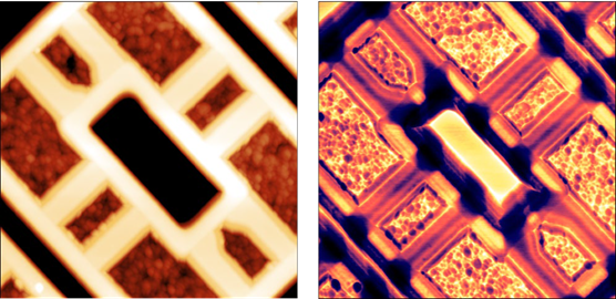
Figure 1. Topography (left), Im (S11) or capacitance (right) of an SRAM sample. Scan size is 10 x 10 μm2. Image Credit: Nanosurf AG
Materials Science
PFM, SMM, EFM, and MFM are used widely in materials science for investigating new materials. PFM has been critical in exploring the piezoelectric properties of polymers, resulting in the advancement of high-performance piezoelectric sensors and actuators. EFM provides insights into the charge-trapping phenomenon in organic semiconductors, enhancing the stability of these materials.
SMM can probe local dielectric properties and has thus been essential in characterizing complicated materials systems, including multiferroics and ferroelectric thin films. This resulted in the development of new multifunctional devices. MFM helps in understanding magnetic domain arrangements and changes. It is also essential for the examination of nanoscale magnetic structures in novel materials.
Energy Industry
C-AFM and SMM have emerged as potent tools in the energy industry. C-AFM has been utilized to evaluate the conductivity and ion transport properties in the solid electrolytes of next-generation lithium-ion batteries.
This played a substantial role in the development of more efficient and safer efficient lithium-ion batteries. Through its ability to assess dielectric properties, SMM contributes to understanding material behavior in actual operating conditions, facilitating the design of more robust and efficient fuel cells.
Life Sciences
Electrical AFM modes, such as SMM and C-AFM, have discovered unique life science applications. C-AFM has been utilized to investigate the electrical conductivity of neurons, improving our knowledge of neural communication at a cellular level and helping with the development of sophisticated neuroprosthetics.
Thanks to its ability to measure local permittivity, SMM has provided novel insights into cellular processes, improving our understanding of biomaterials and biological systems and facilitating the development of advanced treatments and drugs.
Data Storage
Electrical AFM modes such as C-AFM, SMM, and MFM, are important in the development of sophisticated data storage technologies. MFM has been employed to investigate the nanoscale magnetic domains in hard disk drives (Figure 2), resulting in substantial increases in storage density.
C-AFM has been utilized to study the electrical properties of magnetic recording media, while SMM provides unique benefits in the characterization of memory devices because of its ability to probe subsurface features. This has facilitated the development of next-generation high-density storage systems, such as advanced solid-state drives with enhanced reliability and data retention properties.
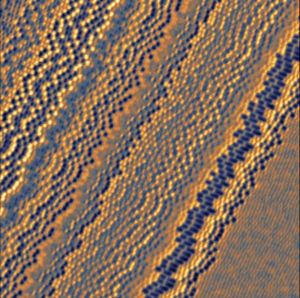
Figure 2. MFM image showing the data stored in a hard disk drive. Hard disc drives remain to be the choice of preference for long-term data storage in servers. MFM is used both during the development of new drives and as part of the quality control process. Image size: 11 x 11 μm2. Image Credit: Nanosurf AG
Understanding the Modes
Conductive Atomic Force Microscopy / Scanning Spreading Resistance Microscopy
C-AFM was first developed at the University of Cambridge in 1993. It assesses the localized electrical properties of a material. In C-AFM, the probe is coated with a conductive material and acts as a nanoscale electrode.
The application of a bias voltage facilitates the flow of a current from the tip to the sample. The current flowing between the probe and the sample is then measured, offering insights into the local electrical conductivity—that is, the resistance of the local tip-sample contact is assessed (Figure 3).
Figure 3. Topography (left) and a C-AFM image (right) of an ITO thin film on glass substrate. Image size: 5 x 5 μm2, current range: 12 nA. Image Credit: Nanosurf AG
In C-AFM measurement a direct current (DC) voltage is applied to the tip and the resulting current is measured. To achieve this, a linear trans-impedance amplifier is used to convert the current into a voltage signal. This type of amplifier can handle up to 4-5 decades of a current within one range.
Some current measurements, such as in semiconductor heterostructures, necessitate greater current ranges—that is, up to 7-8 decades. This can be accomplished using a logarithmic trans-impedance amplifier.
When used with a logarithmic amplifier, C-AFM is referred to as SSRM. The term originates from the early days of the semiconductor industry, and the addition of the word microscopy to the existing measurement of scanning spreading resistance was made when the mode became available in modern AFMs.
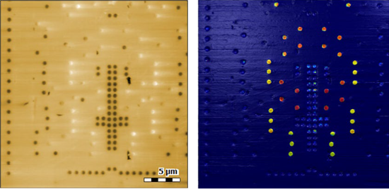
Figure 4. Topography (left) and a C-AFM image (right) of an interconnect structure. The C-AFM image shows different conductivities for different groups of contacts. Image size: 25 x 25 μm2, current range: 1.5 nA. Image Credit: Nanosurf AG
SSRM and C-AFM provide valuable information on solid materials, micro-, and nanoscale electronic devices (Figure 4), conductive polymers, thin films, nanoparticles, biological samples, and nanostructures as small as single molecules.
They also have extensive applications in the solar cell and semiconductor industries for a variety of high-resolution measurements, such as material characterization, semiconductor dopant profiling (Figure 5), and quality control for dielectric films and oxide layers.
An additional type of C-AFM is the quantification of local current-voltage characteristics of the tip-sample contact. These convey information regarding the type of conductivity in the sample, whether it be dielectric, semiconductor, semimetal, or metal.
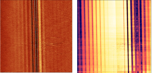
Figure 5. Topography (left) and an SSRM image (right) of a dopant density calibration sample. SSRM image shows different conductivities for regions with different dopant densities. Range of dopant densities: 4x10¹⁵ – 1020 cm-3. Image size: 50 x 50 μm2, current range: 15 μA. Image Credit: Nanosurf AG
Electrostatic Force Microscopy
EFM measures the electrostatic force acting between the probe and the sample, unveiling information about charge distribution and local surface potential.
To achieve this, a probe coated with an electrically coated material is typically oscillated at its resonance frequency without making contact with the sample. In these conditions, the oscillating cantilever is sensitive to long-range electrostatic force gradients.
Fluctuations in the potential difference between the tip and sample result in a change in the cantilever’s resonance frequency. This causes an alteration in the phase response at the excitation frequency. EFM is especially valuable in comprehending phenomena related to charge trapping and charge transport in semiconductors and dielectric materials.
Kelvin Probe Force Microscopy
KPFM measures the contact potential difference (CPD) between the sample and the conductive AFM probe. This refers to the difference in their work functions, which provides information about the surface potential of the sample and thus valuable insights into the sample’s electronic structure.
KPFM typically functions by imaging the sample in dynamic mode and exciting the cantilever probe electrically at another frequency to determine the CPD. A second feedback loop evaluates the mechanical cantilever response to the electrical AC excitation. This controls the DC tip bias and therefore determines the CPD between the sample and tip by reducing the electrostatic forces acting between them.
KPFM thus enables mapping the local CPD and, consequently, the work function across the surface of the sample. This serves as an important tool for investigating material distribution (for instance) that cannot be acquired by topographic imaging, corrosion, semiconductor materials, thin films, and two-dimensional (2D) materials. Figure 6 highlights an example of semi-fluorinated alkanes, which are barely visible in topographic imaging but can be easily identified by KPFM.
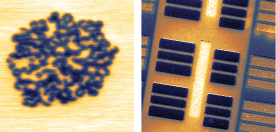
Figure 6. KPFM images of a self-assembly of semi-fluorinated alkane molecules F(CF2)14(CH2)20H (F14H20) on mica (left) and an SRAM sample showing regions with different carrier doping (right). Both images were recorded by single pass AM KPFM on 2nd eigenmode. Image sizes: 2 x 2 μm2 (left) and 40 x 40 um2 (right). Image Credit: Nanosurf AG
In semiconductor materials, areas with different dopant levels appear to have different surface potential (shown in Figure 6). KPFM can thus be utilized to identify materials, assess the impact of treatments on conductivity, pinpoint defects (such as impurities embedded within the substrate), or recognize components of a circuit that are not electrically connected.
KPFM can also be used to study novel 2D materials. Applications include characterizing chemical doping in graphene used for chemical sensors, determining the number of layers, screening the electrical properties of stacked 2D materials and interactions with substrates, and simply assessing the grown materials' purity.
The MoS2 flakes depicted in Figure 7 look very similar at first glance, but KPFM imaging uncovers subtle differences in the CPD in the center of the flakes, possibly lattice defects or impurities.
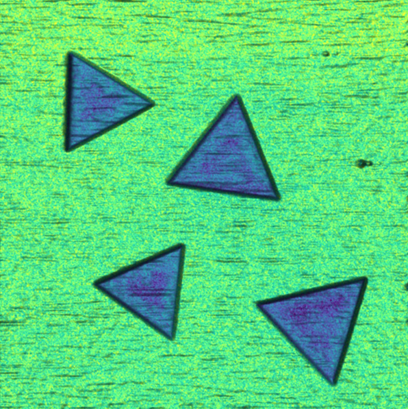
Figure 7. KPFM image showing 2D crystals of MoS2 on silicon oxide. Image was done by off-resonance single pass AM KPFM. Image size: 42 x 42 μm2. Image Credit: Nanosurf AG
Piezoresponse Force Microscopy
PFM is a potent method utilized to assess the piezoelectric response of materials. Piezoelectric materials exhibit a fascinating property: when subjected to mechanical deformation, they generate a voltage; when exposed to an electrical field, they deform.
Piezoelectric materials have diverse applications spanning from biomedicine (such as biosensors, ultrasound, or auditory) to advanced electronics (such as energy production, sonar equipment, or data storage).
To investigate piezoelectric materials at the nanoscale, PFM uses the reverse piezoelectric effect. In PFM, an alternating voltage (VAC) is applied between the conductive tip of an AFM probe and the sample. This causes sample deformation.
The subsequent alteration in the probe's deflection at the frequency of the VAC is measured, offering valuable insights into the amplitude and phase of the piezoelectric response. Amplitude reports the amount of material’s extension in the sample. Phase indicates the orientation (polarization) of a material within a sample.
This characteristic of PFM is widely utilized in the examination of piezoelectric thin films, ferroelectric materials, and advanced actuator and sensor materials. For instance, the practical applications of PFM are evident in the investigation of numerous materials.
Lead zirconate titanate (PZT), a common piezoelectric material, and lithium niobite (LiNbO3), an optically transparent material extensively utilized in mobile phones and piezo sensors, have been comprehensively studied with PFM.
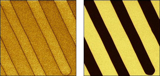
Figure 8. CR-PFM on LiNbO3: PFM amplitude (left) and PFM phase (right). In the PFM amplitude image, the piezoelectric domain boundaries are clearly visible while the PFM phase image indicates the polarization direction of the domains. Image size: 30 x 30 μm2. Image Credit: Nanosurf AG
Figure 8 indicates an example of periodically poled LiNbO3 imaged in PFM utilizing the contact resonance of the cantilever to augment the piezoelectric response of the material. VAC is applied at the cantilever’s contact resonance, enabling the use of smaller VAC or the examination of weakly responsive or thin materials.
Deformation in response to VAC is negligible at the domain boundaries, and therefore the amplitude image unveils these structures. The phase image provides information about the orientation of the piezoelectric domains. Opposite domain orientation triggers the phase signal to alter by 180° as depending on the orientation, the sample deformation is counter-phase or in-phase or to VAC.
In ferroelectrics. switching spectroscopy (SS) PFM is utilized to probe the switching voltage for the electrical polarization. VAC is applied to assess the piezoresponse, typically at or near the frequency of the contact resonance.
To quantify remanent polarization, the static bias voltage (VDC) undergoes cycling between “off” (VDC=0) and “on” states, where the voltage in the “on” state voltage is increased at each switching event.
The voltage applied in the “on” state influences the local polarization, whereas the polarization measured in the “off” state reflects the remanent state polarization, which may differ from the state when voltage is applied.
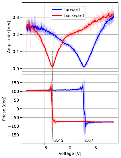
Figure 9. Highly reproducible (11 repetitions) SS-PFM measurement on a BaTiO3 thin film sample at the contact resonance frequency. The amplitude and phase for all measurements were plotted for the voltage “off” state, showing the remanent polarization, with the thick curve representing the average of those curves. Image Credit: Nanosurf AG
This process enables the determination of the switching voltage—that is, the voltage at which the remanent state polarization is reversed. Figure 9 depicts typical phase and amplitude responses of an SS PFM study. The direction of the VDC bias change determines the switching voltages, which are marked by the 180° phase changes in the phase curves and the minima in the amplitude curves.
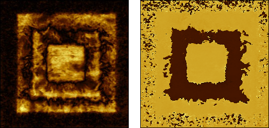
Figure 10. PFM amplitude (left) and phase (right) of P(VDF-TrFE) thin film after applying DC sample bias of 40 V, 40 V, and 40 V during consecutive scanning of 3x3 μm2, 2x2 μm2, and 1x1 μm2 areas respectively. Amplitude range: 10 pm; Phase range from -90° to 90°. Sample courtesy: Joanneum Research Forschungsgesellschaft mbH, Austria.
Achieving the coercive field for switching may necessitate bias voltages that surpass the voltage levels available in the AFM scan head. In these instances, a high-voltage amplifier is connected to a user output of the AFM controller, and bias voltages (VDC) up to ±200 V can be applied (as shown in Figure 10).
The excitation voltage (VAC) can also be applied through the high-voltage amplifier to enhance the signal-to-noise ratio of weak piezoelectric properties. The specimen must be stable under high voltage to conduct HV-PFM. Electronics must not be exposed to the high voltages applied to the sample, as to prevent damage to electronic equipment or physical harm to the operator.
Using PFM, researchers can obtain valuable insights into the piezoelectric properties of materials, allowing for a more comprehensive understanding of their behavior. Therefore, PFM contributes to the advancement of numerous fields (such as device fabrication, materials science, and nanotechnology).
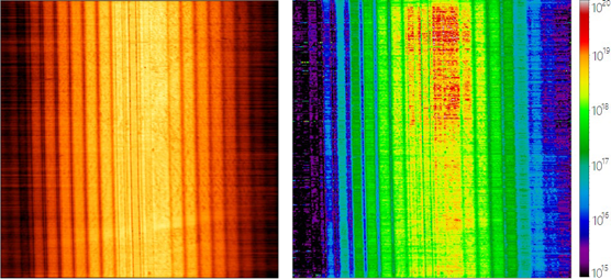
Figure 11. S11 amplitude (left) and dopant density map (right) of an Infineon SCM calibration sample with dopant densities in a range of 4x10¹⁵ – 1020 cm-3. Scan size is 50 x 50 μm2. Image Credit: Nanosurf AG
Scanning Microwave Microscopy
In SMM, a microwave signal is transmitted via microscopy (SCM), making it a more sensitive and modern technology compared to scanning capacitance microscopy SCM. Similar to C-AFM, SMM can be applied to a variety of materials, spanning from dielectrics to metals. Its applications extend from semiconductors and materials research to the field of biological sciences.
The most significant application of SMM, in conjunction with SSRM and C-AFM, is failure analysis and quality control in semiconductor structures (shown in Figures 1 and 2). Unlike SSRM or C-AFM, SMM will exhibit excellent contrast, even when the structures of interest are concealed by an insulating oxide layer. This demonstrates the subsurface imaging capabilities of SMM. Consequently, sample preparation and imaging reproducibility for SMM are simpler than that for SSRM or C-AFM.
For calibrated measurements, such as dopant density calculations, SMM is more robust than SSRM or C-AFM. However, to successfully process SMM images, basic knowledge of microwaves and the physics of the measurement is required.
SMM operates in two distinct modes: the S11 measurement (described above), and the dS/dV measurement, in which the S11 parameter is modulated via an external AC voltage. This mode is valuable when investigating non-linear materials, such as semiconductors or piezoelectrics. For instance, in semiconductor heterostructures, a phase flip in the dS/dV signal indicates an alteration of the dopant type—that is, n or p (as shown in Figures 12 and 13).
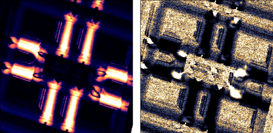
Figure 12. dS/dV amplitude (left) and phase (right) or an SRAM sample. The bright regions in the amplitude image are the p-type conducting channels. Image size: 11 x 11 μm2. Image Credit: Nanosurf AG
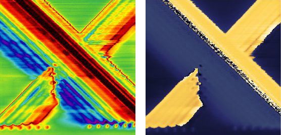
Figure 13. dS/dV amplitude (left) and phase (right) of an SCM calibration sample. The amplitude non-linearly depends on dopant density, with a maximum around 1017-1018 cm-3, and the phase change indicates the change of the type of dopants – n or p. Image size: 40 x 40 μm2. Image Credit: Nanosurf AG
Magnetic Force Microscopy
MFM utilizes AFM probes coated in magnetic material and a dual-pass imaging mode to detect the stray magnetic field above the sample surface. The surface topography of the specimen is measured during the first pass in dynamic mode. The dominant force when closer to the surface is the van der Waals force, and while electrostatic and magnetic forces are present, they are not as strong.
In the second pass at a lift height, the probe scans the surface, tracking the topography reported in the first pass. At the lift height, the magnetic and electric forces do not decay as rapidly (1/r2 and 1/r3, respectively) compared to the van der Waals force.
Measurement of the phase shift between the AC excitation signal and the recorded AC cantilever deflection enables the acquisition of an image proportional to the gradient of the stray magnetic field, enabling the visualization of the edges of the magnetic domains.
MFM can be used to investigate the magnetic behavior of electrical steel. Electrical steel has numerous applications, such as in transformers for electricity transmission (depicted in Figure 14), the study of thin films of magnetic coatings in magnetic hard discs (shown in Figure 2, right), or the investigation of magnetization within microscale or nanoscale magnets (Figure 15).
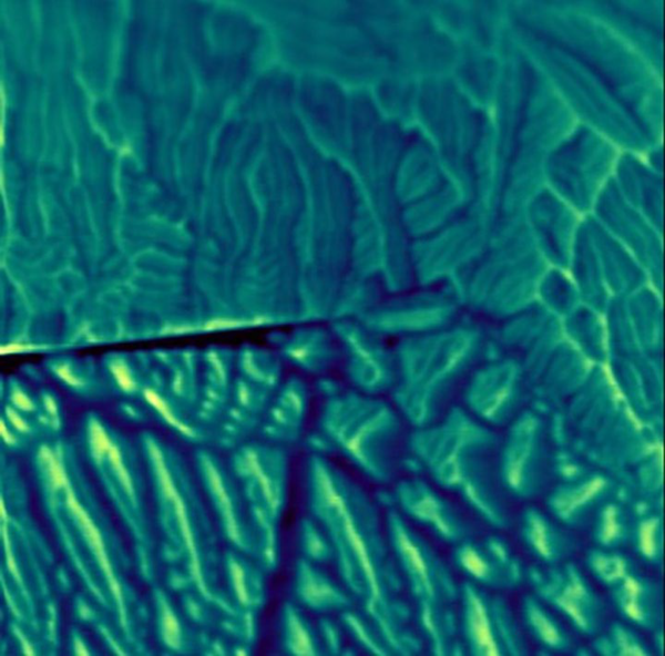
Figure 14. Left: MFM image, showing phase contrast, generated by the stray fields of magnetic domains in electrical steel. By varying in-plane magnetic field, it is possible to study the evolution of magnetization, and thus understand the origin of losses in electrical transformers or motors. Image size: 100 x 100 μm2. Image Credit: Nanosurf AG
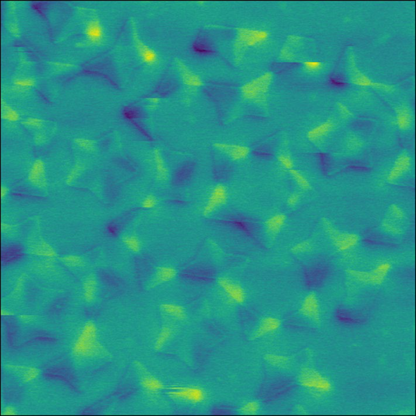
Figure 15. MFM image of stray magnetic fields between the nanomagnets in artificial spin ice. Arrays of nanomagnets are being used in neuromorphic devices to mimic how the brain operates in order to increase computation capabilities without scaling up power consumption. MFM, and variable magnetic field sample holder were used to study the evolution of these magnetic structures and how they interact with each other. Image size: 13 x 13 μm2. Image Credit: Nanosurf AG
Conclusion
Electrical AFM modes, including the recent addition of SMM, have become potent tools for nanoscale analysis, offering in-depth insights into the electrical properties of materials. They have numerous applications across diverse industries, highlighting their importance in developing and manufacturing a wide range of products and technologies.
As AFM modes continue to develop, they hold the potential to unlock new possibilities in nanoscale analysis, paving the way for future advancements in various fields. Continuous refinement and innovation of these techniques offer the prospect of achieving a more comprehensive understanding of materials and devices at the nanoscale. This may result in significant breakthroughs that could transform our lives in ways that are yet to be fully realized.

This information has been sourced, reviewed and adapted from materials provided by Nanosurf AG.
For more information on this source, please visit Nanosurf AG.