Modern advanced packaging processes and shrinking semiconductor device sizes mean that it is vital to consistently eliminate sub-20 nm defects and surface contaminants. To do this effectively, the molecular identity of a defect or contaminant must be accurately discerned.
Traditional analytical survey tools such as XPS, ToF-SIMS, or SEM/TEM EDX can detect defects as small as 20 nm, but these tools may struggle to clearly identify the contaminating source of defects, particularly where these are organic.
Identifying organics at this scale is challenging because conventional analytical tools tend to lack the required spatial resolution, or these tools may only provide elemental information.
There is the potential to fill this analytical gap with infrared photo-induced force microscopy (IR PiFM), allowing users to identify specific chemical compounds with nanometer-scale resolution. IR PiFM combines a non-contact AFM with IR spectroscopy, enabling the concurrent acquisition of topographical and chemical information at the nanoscale.1
PiF-IR spectra match FTIR spectra for a given material, meaning it is possible to leverage existing IR libraries to identify defects analyzed with IR PiFM.
PiFM’s capacity for sub-5 nm spatial resolution means that it is possible to decompose a multi-component defect into pure components via the multivariate data analysis of PiF-IR spectra from several regions of a defect.
Results and Discussion
Inorganic and Organic Nanoparticles
A particle was detected, as shown within the red dotted circle of Figure 1. This particle is approximately 3 nm in height and appears to be around 20 nm wide laterally.
The AFM tip is not infinitely sharp, however, meaning that the particle is most likely a sphere with a diameter of around 3 nm. The particle’s width is likely dilated due to the AFM tip’s radius of curvature (approximately 20 nm).
The blue PiF-IR spectrum acquired on the particle matches the orange FTIR spectrum for silica, as listed in the Wiley IR library.2 This example demonstrates the relative ease of employing PiF-IR spectra in confidently identifying unknown nanoparticles.
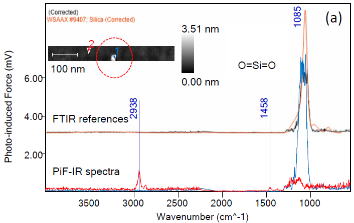
Figure 1. PiF-IR spectrum from a 3 nm particle found on a silicon surface is identified to be a silica particle by searching the Wiley KnowItAll IR library. Image Credit: Molecular Vista
Figure 2 shows a further beneficial example of using PiF-IR spectroscopy and PiFM imaging to directly identify materials at the nanoscale. The sample in this instance is a 20 nm polystyrene (PS) particle deposited onto a mica surface.
The figure’s inset features AFM topography and PiFM images. It is important to note that in this context, PiFM images are chemical absorption maps showing how strongly the material absorbs light of a given wavenumber. In this instance, light at 1492 cm−1 highlights the PS particle, while light at 1025 cm−1 highlights the mica surface.
The lateral size in this example has also been dilated in the topography due to the tip’s radius of curvature. This means that the particle’s height is the most useful measurement of its diameter.
In the example presented here, the red PiF-IR spectrum acquired on the nanoparticle and the blue spectrum on the surface closely match the FTIR spectra for PS (orange) and mica (green).
In the case of PS, every prominent FTIR peak is clearly visible in the PiF-IR spectrum acquired on the particle, while additional peaks shown between 1100 cm−1 and 1350 cm−1 could be due to the presence of a surfactant layer that had been used to disperse the nanoparticles.
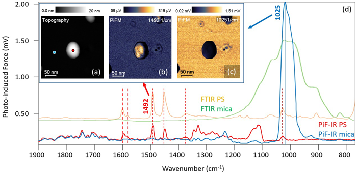
Figure 2. AFM topography, PiFM images, and PiF-IR spectra acquired on a 20 nm polystyrene nanoparticle. Image Credit: Molecular Vista
Ultra-Thin Residues
Surface contamination is another common issue in semiconductor processes, alongside particulate defects. For example, dirty surfaces may interfere with bonding processes in contemporary advanced packaging processes.
It is difficult to detect the existence of these monolayers, let alone identify them. Inferences are often made on the surface of a sample based on unreliable information, such as water contact angle measurements. Thankfully, it is possible to use PiF-IR spectra and PiFM images to directly detect and characterize monolayers.
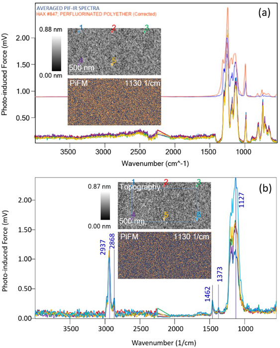
Figure 3. (a) five PiF-IR spectra of a supposedly blank Si wafer, showing some fluorocarbon contamination. (b) five more spectra on the same wafer post-plasma cleaning. Image Credit: Molecular Vista
The bottom section of Figure 3a shows five PiF-IR spectra that had been acquired on an otherwise clean wafer from a storage container. The spectra’s relatively repeatable nature suggests a homogeneous surface chemistry, even though these had been acquired from five different locations.
A strong peak is shown at ~1250 cm−1 in addition to the silicon oxide peak at 1130 cm−1. Averaging these spectra (blue spectrum) and performing a search in the Wiley IR library reveals a match to the FTIR spectrum of perfluoropolyether (PFPE) (shown in orange). The sample’s ultra-flat topography suggests that the PFPE would form a conformal monolayer that uniformly covers the surface in this instance.
It is important to note that even though the surfaces in Figure 3a and Figure 3b are contaminated with different molecules, the silicon substrate’s microstructure remains the same. This highlights the thinness of the contaminant layers.
The PiFM image at 1130 cm−1 also highlights the silicon oxide, demonstrating increased contrast variations across the surface following the plasma cleaning versus the original. This is consistent with the varying peak strengths noted in the spectra, suggesting the presence of subtle differences in the oxide between locations.
This example highlights the usefulness of nanoscale IR measurements in investigating surface preparations. Without PiF-IR spectra, it would be impossible to determine where surface contaminants like these may originate.
The cleanliness of copper surfaces must be determined as they are prepared for hybrid bonding. This example is increasingly relevant because hybrid bonding is gaining interest as a potential replacement for thermal compression bonding in advanced packaging applications requiring higher interconnect density.
Successful hybrid bonding requires an extremely flat, clean, smooth, and hydrophilic dielectric surface that is properly terminated with Si-OH bonds able to instantly bond together upon contact at 25 °C.
To ensure good metal-to-metal bonds, Cu surfaces must also be free of organic contaminants and carbides that could prevent true Cu interfacial grain growth.
Benzotriazole (BTA) is used as an inhibitor to protect recessed copper, and this is known to react with copper ions to form a thin Cu(II)-BTA polymer on the copper surface that is difficult to remove.3
Figure 4 features averaged PiF-IR spectra of four copper surfaces:
- As electroplated
- After the electroplated copper has been treated by BTA
- Following the CMP process of electroplated copper
- After Ar ion cleaning, following the CMP process
The as-electroplated copper (Figure 4a) shows a peak at around 730 cm−1, attributable to copper oxide. Two peaks at ~795 cm−1 and 755 cm−1 appear when the copper is treated with BTA (Figure 4b), attributable to the C-H stretching vibration of the benzene ring in BTA. These peaks clearly indicate the formation of Cu-BTA polymer.3
The presence of these two peaks can also be observed in the copper sample undergoing a CMP process (Figure 3c), though the peak at 795 cm−1 appears as a shoulder of a new peak.
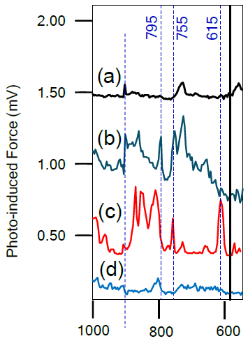
Figure 4. Averaged PiF-IR spectra for different copper surfaces. (a) as electroplated, (b) after the electroplated copper is treated by BTA, (c) after the CMP process of electroplated copper, and (d) after Ar ion cleaning following the CMP process. Image Credit: Molecular Vista
The prominent new peak observable at ~615 cm−1 is commonly associated with Cu2O4.
The copper surface was observed to be mostly clean after the same sample had been cleaned via Ar ion beam (Figure 4d). A small peak at ~805 cm−1 was observed, however, which may be due to the oxide peak associated with the AFM tip.
It is also important to note that the sharp feature seen at ~905 cm−1 in all spectra is an artifact of laser power normalization, meaning that this can be safely ignored.
Other surface-sensitive techniques such as XPS can be employed in order to determine the presence of the Cu-BTA complex, but PiFM offers a distinct advantage in that its spatial resolution facilitates the examination of individual copper pads, which are increasingly less than 1 µm in size.
Conclusion
IR PiFM can be used to chemically identify sub-20 nm defects in organic or inorganic materials. Its capacity to efficiently detect and characterize monolayer residues without contaminating the sample affords IR pIFM a significant advantage over techniques like SEM analysis, which generally contaminate samples with carbon deposits.
It is also possible to leverage IR PiFM to sensitively check post-CMP residues, even on individual copper pads for Cu-Cu hybrid bonding applications. IR PiFM’s ability to assess Si-OH bonds’ density on SiO2 surfaces after cleaning processes is also important to note.
IR PiFM capabilities are available on instruments supporting up to 12” wafers. A range of automation features is also available, including automated defect analysis based on KLARF coordinates.
References and Further Reading
- Nowak, D., et al. (2016). Nanoscale chemical imaging by photoinduced force microscopy. Science Advances, 2(3). https://doi.org/10.1126/sciadv.1501571.
- Wiley Science Solutions. (2025). KnowItAll IR Spectral Database Collection - Wiley Science Solutions. (online) Available at: https://sciencesolutions.wiley.com/solutions/technique/ir/knowitall-ir-collection/.
- Wang, Q., et al. (2019). Study on Infrared Spectrum Detection and Analysis of BTA Residual after Copper CMP. 2022 China Semiconductor Technology International Conference (CSTIC), (online) pp.1–3. https://doi.org/10.1109/cstic.2019.8755680.
- Chen, A., et al (2009). Controlled growth and characteristics of single-phase Cu2O and CuO films by pulsed laser deposition. Vacuum, 83(6), pp.927–930. https://doi.org/10.1016/j.vacuum.2008.10.003.

This information has been sourced, reviewed and adapted from materials provided by Molecular Vista.
For more information on this source, please visit Molecular Vista.