The Vista 200 provides precise nano-chemical analysis with sub-5 nm resolution and exceptional stability.
Vista 200: Power Meets Precision
Controlled Environment
A metal enclosure lined with Mylar-wrapped insulating foam ensures acoustic isolation and maintains temperature stability within 0.1 °C, while also being compatible with cleanroom environments.
Clear Signal
The fully enclosed light path enhances infrared transmission by eliminating atmospheric interference from water vapor, significantly boosting the signal-to-noise ratio (SNR).
Exceptional AFM Performance
The AFM delivers exceptional performance. It is equipped with a 120 µm XY scanner, a 12 µm sample Z scanner, and integrated vibration isolation. The high-bandwidth dual-Z feedback system enables true non-contact AFM for IR PiFM.
Ultimate Spectro-Nanoscopy
Photo-induced force microscopy (PiFM) and photo-induced force infrared (PiF-IR) spectroscopy represent the forefront of nano-IR techniques. Non-destructive, non-contact, and capable of monolayer sensitivity, this instrument sets the standard in its class.
Reliable Spectra
Active beam steering ensures spectral consistency across the entire sample, while the non-contact AFM design prevents cross-contamination.
Dynamic Laser Control
An integrated optical multiplexer automates polarization and normalization, providing seamless laser control and enabling effortless light source selection with perfect beam co-alignment.

Image Credit: Molecular Vista
Download the Brochure for More Information
Semiconductor-Specific
Streamlined Processes
The included data analysis software enables the team to quickly transform measurements into presentation-ready results. Seamless integration with the data acquisition platform delivers real-time insights when users need them most.
A flexible scripting API supports custom workflows, and the open file formats ensure easy compatibility with third-party software.
Made for the Samples
Customize the setup with a vacuum chuck featuring magnetic mounts or an EUV mask holder—ideal for 4-, 6-, or 8-inch wafers.
Powerful Yet Non-Destructive
PiFM operates in true non-contact mode, preserving the integrity of the pristine samples and keeping the AFM tip clean.
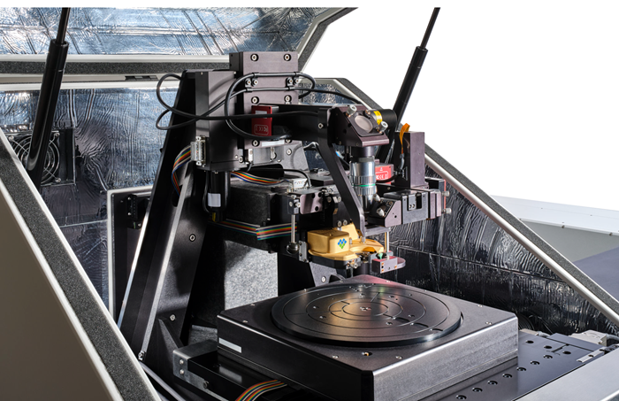
Image Credit: Molecular Vista
Built for Industry
Maximize Efficiency Minimize Disruption
The 300 mm-wide sample access door minimizes thermal disturbances leading to drift while enabling maximum throughput. Thanks to the forward-moving stage and user-friendly head mount, both the tip and sample can be quickly swapped without opening the full enclosure.
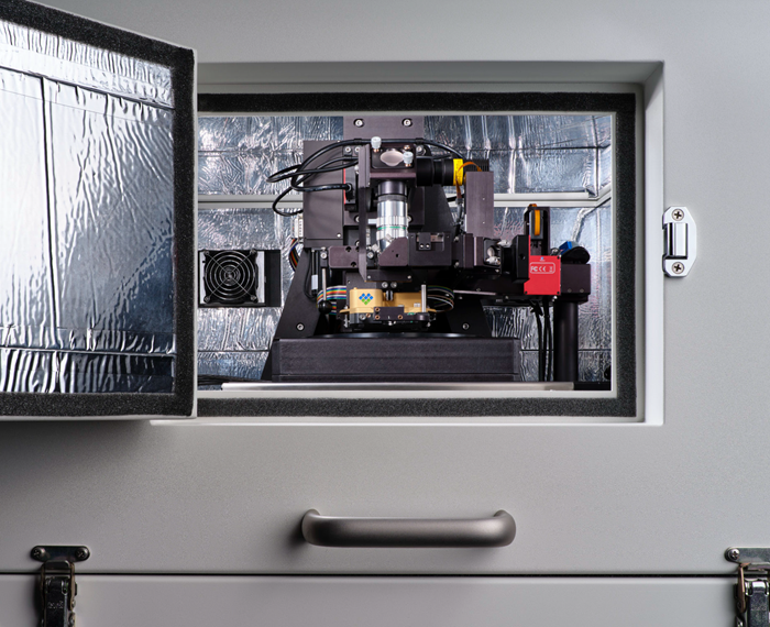
Image Credit: Molecular Vista
Scientific Principles PiFM and PiF-IR

Figure 1. A pulsed and tunable IR laser is focused onto the apex of a metal-coated AFM tip. The laser is modulated at a frequency carefully calculated based on the resonance frequencies of the cantilever. Image Credit: Molecular Vista
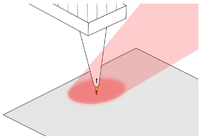
Figure 2. The metal-coated AFM tip acts as an antenna, creating a highly local enhanced field (yellow). This field locally polarizes the sample, resulting in an attractive force whose magnitude depends on the absorption strength of the sample. Image Credit: Molecular Vista
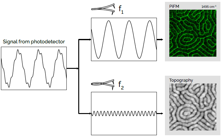
Figure 3. One resonance of the cantilever is used to detect the PiFM signal. Simultaneously, another resonance is used to collect the standard AFM topography and phase in a non-contact manner (no tip/sample contamination). Image Credit: Molecular Vista
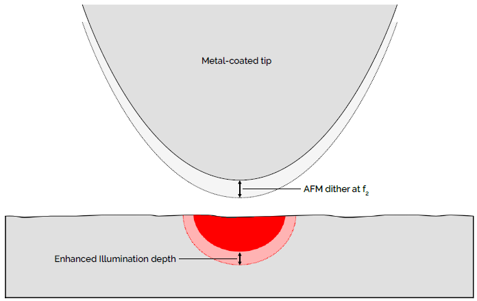
Figure 4. The depth of the tip-enhanced illumination depends heavily on the spacing between the tip and the sample. By detecting the attractive forces in non-contact mode, the measurement is made extremely sensitive, capable of detecting monolayers of material. Image Credit: Molecular Vista
The Result
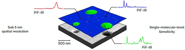
Figure 5. PiF-IR nanoscale spectra are made by measuring the strength of the attractive photo-induced forces as a function of wavenumber. PiFM chemical maps are created by scanning the surface with a fixed-wavenumber to measure absorption strength as a function of position. The color layer over the AFM topography is combined with three fixed-wavenumber PiFM images. Image Credit: Molecular Vista
Download the Brochure for More Information
PiFM Chemical Mapping
Reveal Hidden Structure in Color
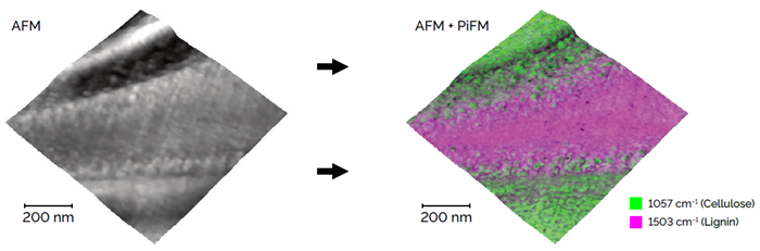
Figure 6. 3D visualization of the AFM topography of a cell wall from an ultra-thin cross-section of spruce wood. An overlay of two PiFM images shows the chemical composition of the surface where lignin and cellulose mix. This PiFM overlay reveals how the materials are distributed and how some of the topographic features are related to the local chemistry. Scan dimensions: 1 µm × 1 µm × 0.034 µm. Image Credit: Molecular Vista
Sub-5 nm Spatial Resolution
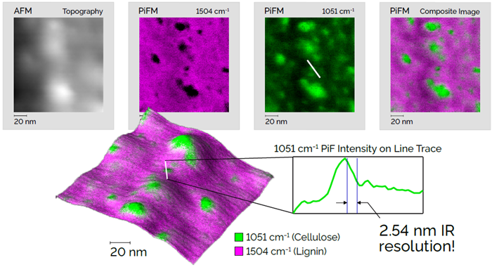
Figure 7. A zoomed-in region of the spruce wood cell wall. At only 150 nm square, this scan area is over 50 times smaller than in figure 6. PiFM images show the chemical distribution of lignin and cellulose on the surface. A line trace plotting the intensity of the data in the green image shows an IR spatial resolution of less than 5 nm. Notice how the PiFM images bring the topography alive with precise chemical detail while the topography itself is unremarkable. Scan dimensions: 150 nm × 150 nm × 10.5 nm. Image Credit: Molecular Vista
PiF-IR Nano-Spectroscopy
Single-Molecule-Level Sensitivity
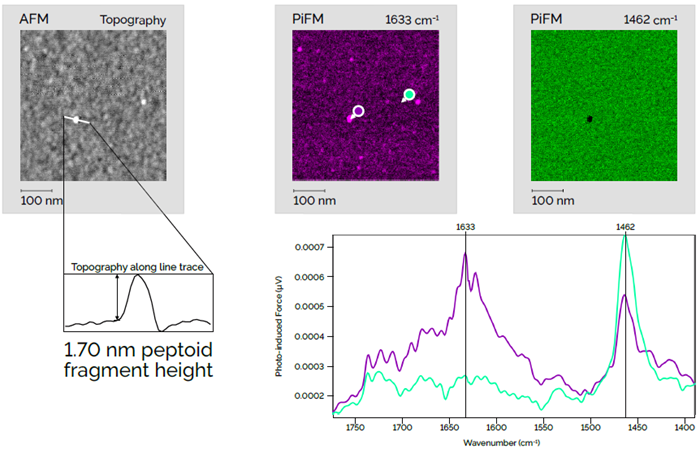
Figure 8. This sample was intended to be a uniform monolayer of peptoid molecules; however, initial PiF-IR analysis indicated that actual peptoid coverage was very sparse. Therefore, a PiFM image was taken at 1633 cm−1, which should highlight any peptoid molecules present. This image reveals tiny peptoid fragments on the surface. A PiF-IR spectrum taken on one of those points shows the characteristic peak at 1633cm−1 despite the peptoid fragment being only 1.7 nm tall! The black spot in the green PiFM image shows that the fragment is sitting on top of the substrate material. Scan dimensions: 500 nm × 500 nm × 1.7 nm. Image Credit: Molecular Vista
Excellent Agreement With FTIR
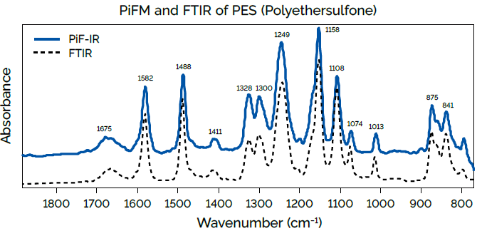
Figure 9. On homogeneous samples, PiF-IR spectra agree with FTIR extremely well. Image Credit: Molecular Vista
Analyze Organic and Inorganic Materials
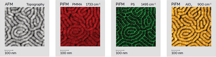
Figure 10. Both organic and inorganic samples can be analyzed equally well using PiFM and PiF-IR. Here, a PS-b-PMMA block copolymer has undergone sequential infiltration synthesis to produce aluminum oxides in the PMMA block. The sample was exposed to a vapor of trimethyl aluminum, which should only react with carbonyl groups in the PMMA. Subsequent exposure to water vapor converts the trimethyl aluminum into aluminum oxide. PiFM analysis after this process confirms the block-selective infiltration by the presence of a new broad peak from 800 to 1100 cm−1 (not shown). A PiFM image taken at 900 cm−1 (yellow image) highlights the infiltrating alumina in the PMMA blocks, demonstrating the exceptional resolution of PiFM chemical mapping even on inorganic samples. Scan dimensions: 500 nm × 500 nm × 5.5 nm. Image Credit: Molecular Vista
Orientation Discrimination
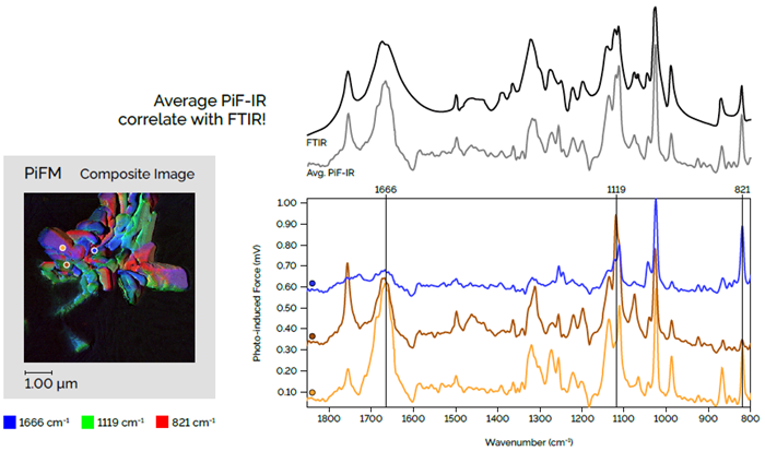
Figure 11. Similar to polarized FTIR, PiF-IR spectra are orientation sensitive due to the tip-enhanced field. The PiF-IR spectra above were acquired at different crystal faces on a vitamin C sample. They exhibit the local IR bands associated with the specific crystal faces. The average of these three distinct local PiF-IR spectra compare nicely with the bulk FTIR spectrum, which is the equivalent of an ensemble average of billions of PiF-IR spectra. Scan dimensions: 640 nm × 640 nm × 1025 nm. Image Credit: Molecular Vista
Download the Brochure for More Information
Comparisons
Comparing Surface Analytical Techniques
Table 1. PiFM & PiF-IR bring molecular analysis to the realm of true nanoscale resolution, providing both IR absorption spectra and chemical mapping with sub-5 nm spatial resolution and monolayer sensitivity, complementing XPS or ToF-SIMS in any high-end lab. *For SEM and TEM, EDS measurements are not as high resolution as is possible for imaging. Source: Molecular Vista
| |
PiFM &
PiF-IR |
Raman |
FTIR |
TOF-
SIMS |
XPS |
TXRF |
SEM/
EDS |
TEM |
Auger |
Species
Detected |
Molecular |
Molecular |
Molecular |
Molecular |
Molecular |
Elemental |
Elemental |
Elemental |
Elemental |
Chemical
Mapping |
Yes |
Yes |
Yes |
Yes |
Yes |
Yes |
Yes |
Yes |
Yes |
Lateral
Resolution |
Sub 5
nm |
> 0.5
μm |
> 10
μm |
100
nm |
Sub 5
μm |
~10
mm |
1 nm
*0.5 μm
EDS |
0.2 nm
*1 – 20 nm
EDS |
8
nm |
Depth
Probed |
20 nm
& bulk |
> 500
nm |
1
μm |
1
nm |
10
nm |
10
nm |
1
μm |
~100
nm |
10
nm |
Vista 200 Specifications
Source: Molecular Vista
| Stage and scanner |
| Sample stage travel |
200 mm × 200 mm square. |
| Scan size |
120 × 120 μm. |
| Dual Z feedback |
12 μm z-scanner with 600 nm fast z-scanner provides both high bandwidth and a large z-range. |
| Physical requirements |
| Table size |
1.2 m × 1.8 m (4 ft × 6 ft) optical breadboard recommended. |
| Enclosure |
300 mm × 200 mm access door minimizes thermal drift. The enclosure is removable without disconnecting cables. |
| Functionality |
| Imaging modes |
Non-contact AFM, PiFM, KPFM, cAFM, nano DMA, FvD (force vs distance) mapping. |
| Spectroscopy modes |
PiF-IR, FvD. |
| PiF Laser options |
QCL (770 – 1840, 1995 – 2395 cm−1), OPO/DFG (590 – 2050, 2250 – 4400, 5000 – 7000 cm−1). |
| Depth Probed |
20 nm in surface mode & greater than 100 nm in bulk mode. |