The new Vista 300 provides automated nano-chemical characterization through advanced AFM-IR technology.
Vista 300: Industry-Leading Usability
Exceptional AFM Performance
Automated features enhance efficiency, but true performance begins with a strong foundation. This AFM delivers exceptional precision by featuring a 90 µm XY scanner, a 12 µm sample Z scanner, and integrated vibration isolation. The high-bandwidth dual-Z feedback system enables true non-contact AFM operation for IR PiFM.
Automatic Alignment
An industry first: critical excitation laser alignment is now handled by computer vision, ensuring optimal performance while significantly reducing time.
Ultimate Spectro-Nanoscopy
Photo-induced force microscopy (PiFM) and photo-induced force infrared (PiF-IR) spectroscopy remain the leading nano-IR techniques. Non-destructive, non-contact, and pioneered by the first company to demonstrate monolayer sensitivity, this instrument continues to advance with powerful new automation capabilities.
KLARF File Navigation
The Vista 300 supports KLARF file navigation, enabling efficient defect detection across the full 300 mm of stage travel.
AutoPiFM
AutoPiFM automates the entire data acquisition process, generating fixed-wavenumber PiFM images for each detected chemical component and capturing PiF-IR spectra for every chemical phase. This streamlines the workflow, as demonstrated by the identification of multiple nanoparticle types in the example.
Automatic Beam Set Up
The advanced beam alignment system ensures the excitation laser consistently targets the focusing optics with precision.
Dynamic Laser Control
An integrated optical multiplexer automatically manages polarization and normalization, enabling seamless laser source selection while maintaining perfect beam co-alignment.
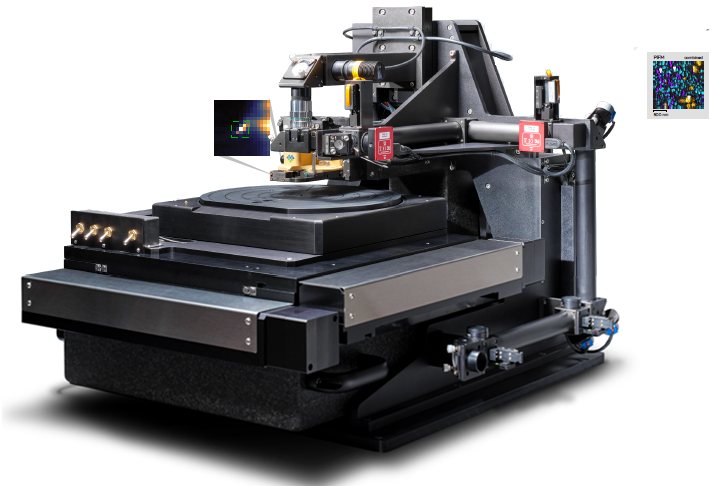
Image Credit: Molecular Vista
Download the Brochure for More Information
A Solid Foundation for Excellent IR
Controlled Environment
The 400 mm-wide sample access door maximizes throughput while minimizing thermal disturbances that could lead to drift. The insulated metal enclosure provides acoustic isolation and maintains temperature stability within 0.1 °C, all while remaining cleanroom compatible.
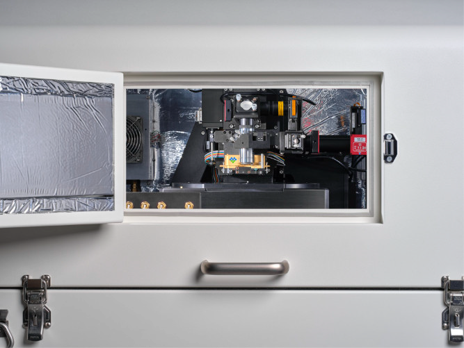
Image Credit: Molecular Vista
Exceptional Stage Access
A forward-moving stage design enables easy sample loading and unloading. With support for samples up to 24 mm in height and 3 kg in weight, the possibilities are limitless.
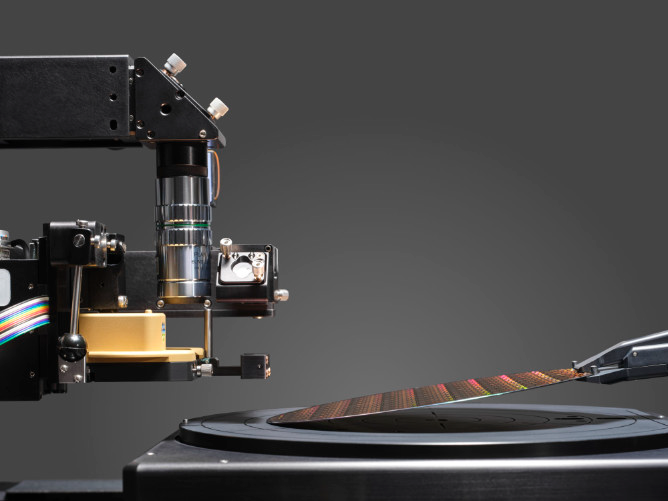
Image Credit: Molecular Vista
Dual-Z Sample Scanning
This is the only 300 mm AFM-IR system on the market that performs scanning in X, Y, and Z directly on the sample. This architecture guarantees stable IR alignment regardless of surface roughness, without compromising the Z-scanner’s bandwidth or travel range.
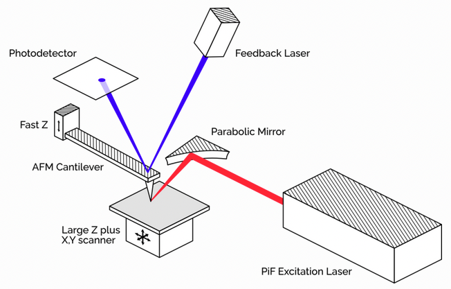
Image Credit: Molecular Vista
Clear IR Signal
A fully enclosed and purged light path maximizes infrared transmission by eliminating atmospheric interference from water vapor, significantly enhancing the signal-to-noise ratio (SNR). Unlike systems that require re-purging, this beam path remains unaffected by sample or probe changes—ensuring immediate access to high-quality spectra.
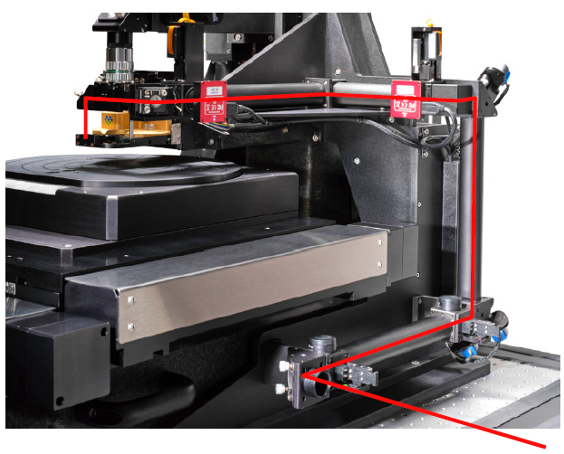
Image Credit: Molecular Vista
Compact Footprint
Thanks to automated beam alignment and an integrated optical multiplexer, the laser system is housed beneath the main instrument, enabling a more compact design without sacrificing performance. The Vista 300 supports up to two lasers, covering the full infrared spectral range (see back cover).
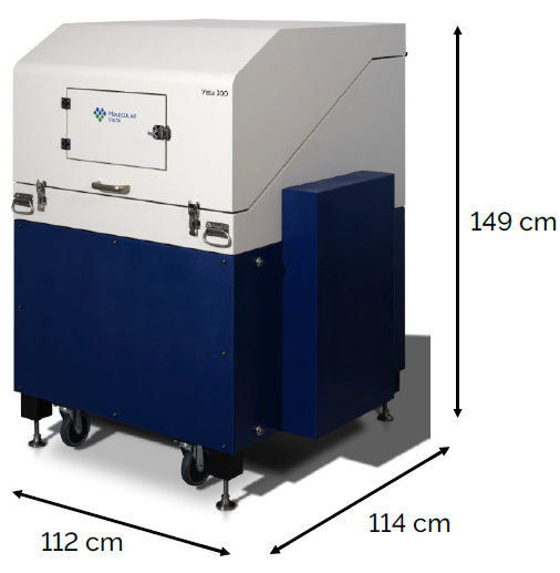
Image Credit: Molecular Vista
Powerful Yet Non‐Destructive
PiFM remains the only true non-contact AFM-IR technique available. The AFM probe never touches the sample, preserving the cleanliness of the sample surface and the tip.
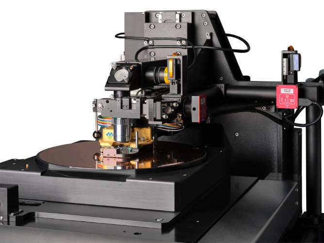
Image Credit: Molecular Vista
Ideal for 12 12-inch wafers
The Perfect Companion
PiFM provides molecular materials, which EDX offers for elemental analysis, enabling precise identification and mapping. While EDX detects elemental composition, PiFM distinguishes individual molecular components. Non-destructive and non-contaminating, PiFM is an ideal complement to techniques such as SEM/EDX, ToF-SIMS, Raman, Auger, and XPS in advanced materials analysis laboratories.
Streamlined Process
A flexible scripting API enables the creation of custom workflows, while open file formats ensure seamless integration with third-party software. The included data analysis tools streamline the process from measurement to presentation-ready results.
Made For the Samples
The system offers a choice between a vacuum chuck with magnetic mounts or an EUV mask holder, making it well-suited for 4-, 6-, 8-, or 12-inch wafers.
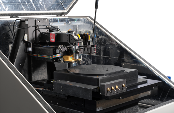
Image Credit: Molecular Vista
Download the Brochure for More Information
Scientific Principles PiFM and PiF-IR
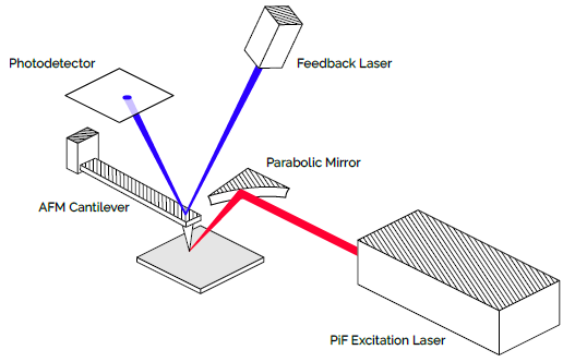
Figure 1. A pulsed and tunable IR laser is focused onto the apex of a metal-coated AFM tip. The laser is modulated at a frequency carefully calculated based on the resonance frequencies of the cantilever. Image Credit: Molecular Vista
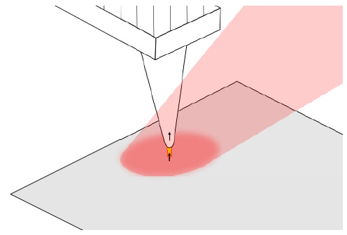
Figure 2. The metal-coated AFM tip acts as an antenna and creates a highly local enhanced field (yellow). This field locally polarizes the sample, resulting in an attractive force whose magnitude depends on the absorption strength of the sample. Image Credit: Molecular Vista
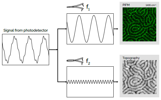
Figure 3. One resonance of the cantilever is used to detect the PiFM signal. Simultaneously, another resonance is used to collect the standard AFM topography and phase in a non-contact manner (no tip/sample contamination). Image Credit: Molecular Vista
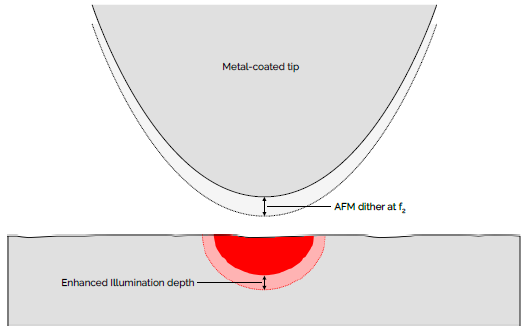
Figure 4. The depth of the tip-enhanced illumination depends heavily on the spacing between the tip and the sample. By detecting the attractive forces in non-contact mode, the measurement is made extremely sensitive – capable of detecting monolayers of material. Image Credit: Molecular Vista
The Result
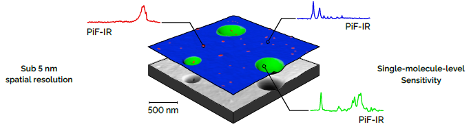
Figure 5. PiF-IR nanoscale spectra are made by measuring the strength of the attractive photo-induced forces as a function of wavenumber. PiFM chemical maps are created by scanning the surface with a fixed-wavenumber to measure absorption strength as a function of position. The color layer over the AFM topography is three fixed-wavenumber PiFM images combined. Image Credit: Molecular Vista
PiFM Chemical Mapping
Reveal Hidden Structure in Color
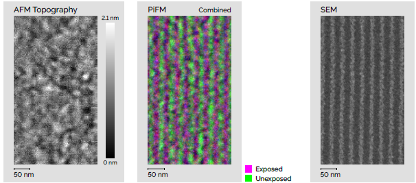
Figure 6. PiFM images are infrared absorption maps which can be used to locate materials. In this example, an EUV photoresist has been exposed with a low dose. The surface is scanned with PiFM before the resist is developed, so the latent image in the photoresist does not appear in the topography. However, two combined PiFM chemical maps can reveal the 16 nm half-pitch structure. Once the resist is developed, the final product can be verified with SEM imaging. Scan dimensions: 300 nm × 600 nm × 2.1 nm. Image Credit: Molecular Vista
Sub-5 nm Spatial Resolution
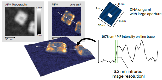
Figure 7. A DNA origami molecule on a silicon substrate. The line trace plots the intensity of the data in the PiFM image (as opposed to the cross-section of the topographic height). The steep rise in absorption intensity at the edge of the molecule shows a spatial resolution of less than 5 nm in the infrared imaging capabilities of Vista 300. Scan dimensions: 200 nm × 200 nm × 3.8 nm. Image Credit: Molecular Vista
PiF-IR Nano-Spectroscopy
Single-Molecule-Level Sensitivity
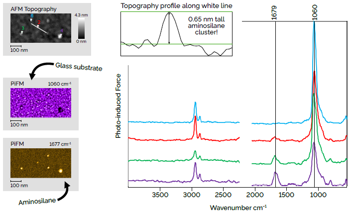
Figure 8. Aminosilane monolayers are a popular for surface functionalization. Conventional wisdom is that the aminosilane will form a uniform monolayer on a clean glass substrate. However, when analyzing some of these functionalized surfaces with PiFM, a different story appears. Instead, it seems that the aminosilane has formed small clusters that are distributed across the surface. The smallest cluster in this image is only 0.65 nm tall! The spectra show that the intensity of the aminosilane peak at 1677 cm−1 grows as the clusters get thicker. Similarly, the intensity of the substrate’s peak at 1060 cm−1 shrinks as that material is hidden under thicker clusters of aminosilane. Scan dimensions: 600 nm × 300 nm × 4.3 nm. Image Credit: Molecular Vista
Excellent Agreement with FTIR
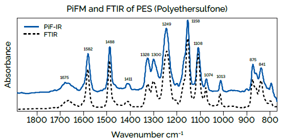
Figure 9. On homogeneous samples, PiF-IR spectra agree with FTIR extremely well. Image Credit: Molecular Vista
Excellent Performance on Inorganic Materials
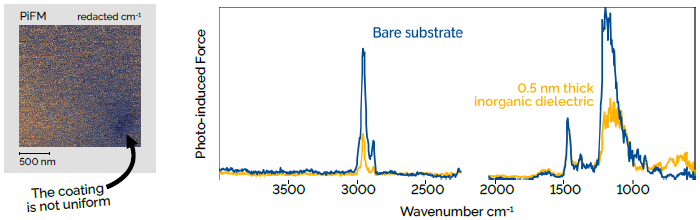
Figure 10. Both organic and inorganic samples can be analyzed equally well using PiFM and PiF-IR. Here, the blue spectrum is a baseline measurement on a clean substrate. Then, a 0.5 nm thick layer of an inorganic high-K dielectric material is applied to the substrate. The gold spectrum shows the chemical changes from the dielectric. Mapping the absorption at a low wavenumber with PiFM shows that, unfortunately, the coating is not uniformly thick. Scan dimensions: 2 µm × 2 µm × 1.1 mV. Image Credit: Molecular Vista
Defect Analysis
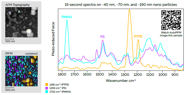
Figure 11. This is a reference sample with different types of nanoparticles. Each of the PiF-IR spectra taken at the markers on the AFM topography image correlates very well with FTIR reference spectra, allowing one to identify the materials as polystyrene (PS), poly methyl methacrylate (PMMA), and polytetrafluoroethylene (PTFE). With nanoparticles ranging in size from about 40 nm up to about 200 nm, this demonstrates how PiFM and PiF-IR can work together for nano-defect analysis. Scan dimensions: 2 µm × 2 µm × 280 nm. Image Credit: Molecular Vista
Download the Brochure for More Information
Comparisons
Comparing Surface Analytical Techniques
Table 1. PiFM & PiF-IR bring molecular analysis to the realm of true nanoscale resolution, providing both IR absorption spectra and chemical mapping with sub-5 nm spatial resolution and monolayer sensitivity, complementing XPS or ToF-SIMS in any high-end lab. *For SEM and TEM, EDS measurements are not as high resolution as is possible for imaging. Source: Molecular Vista
| |
PiFM &
PiF-IR |
Raman |
FTIR |
TOF-
SIMS |
XPS |
TXRF |
SEM/
EDS |
TEM |
Auger |
Species
Detected |
Molecular |
Molecular |
Molecular |
Molecular |
Molecular |
Elemental |
Elemental |
Elemental |
Elemental |
Chemical
Mapping |
Yes |
Yes |
Yes |
Yes |
Yes |
Yes |
Yes |
Yes |
Yes |
Lateral
Resolution |
Sub 5
nm |
> 0.5
μm |
> 10
μm |
100
nm |
Sub 5
μm |
~10
mm |
1 nm
*0.5 μm
EDS |
0.2 nm
*1 – 20 nm
EDS |
8
nm |
Depth
Probed |
20 nm
& bulk |
> 500
nm |
1
μm |
1
nm |
10
nm |
10
nm |
1
μm |
~100
nm |
10
nm |
Vista 300 Specifications
Source: Molecular Vista
| Stage and scanner |
| Sample stage travel |
300 mm × 300 mm square. |
| Scan size |
90 × 90 μm. |
| Dual Z feedback |
12 μm z-scanner with 600 nm fast z-scanner provides both high bandwidth and a large z-range. |
| Physical requirements |
| System dimensions |
Approximately 1.1 m × 1.1 m × 4.9 m (3’ 7.3” × 3’ 7.3”× 5”) |
| Enclosure |
400 mm × 200 mm access door minimizes thermal drift. The enclosure is removable without disconnecting cables. |
| Functionality |
| Imaging modes |
Non-contact AFM, PiFM, KPFM, cAFM, nano DMA, FvD (force vs distance) mapping. |
| Spectroscopy modes |
PiF-IR, FvD. |
| PiF Laser options |
QCL (770 – 1840, 1995 – 2395 cm−1), OPO/DFG (590 – 2050, 2250 – 4400, 5000 – 7000 cm−1). |
| Depth Probed |
20 nm in surface mode & greater than 100 nm in bulk mode. |