The VistaOne offers state-of-the-art spectro-nanoscopy in a compact, user-friendly system. Integrated vibration isolation, advanced environmental controls, and cutting-edge nano-IR techniques—including PiFM and PiF-IR—enable outstanding AFM performance across various laboratory environments.
A versatile suite of accessories designed to support diverse research applications further enhances the sub-5 nm resolution, making it a comprehensive laboratory solution.
The system can be configured for humidity-free measurements using the environmental enclosure and sample transfer system or optimized for transparent substrates with bottom optics. Optional add-ons such as s-SNOM and Raman further expand this instrument's capabilities.
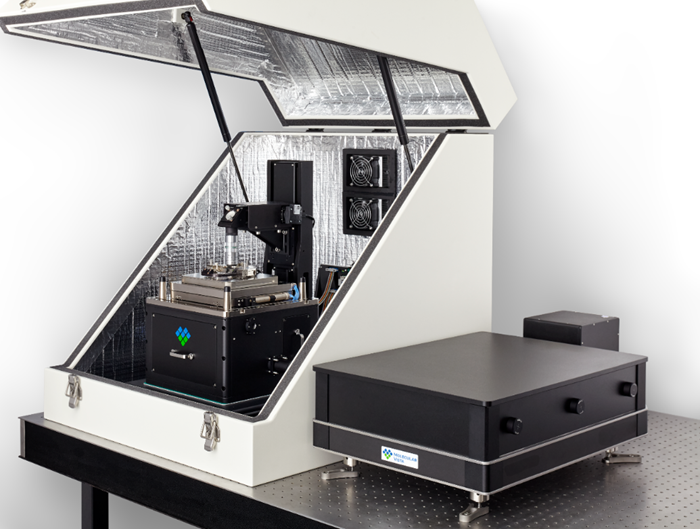
Image Credit: Molecular Vista
Download the Brochure for More Information
Scientific Principles PiFM and PiF-IR
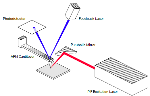
Figure 1. A pulsed and tunable IR laser is focused onto the apex of a metal-coated AFM tip. The laser is modulated at a frequency carefully calculated based on the resonance frequencies of the cantilever. Image Credit: Molecular Vista
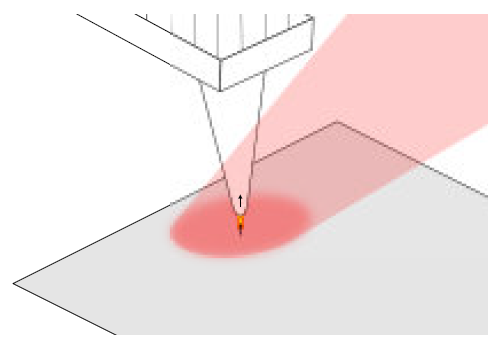
Figure 2. The metal-coated AFM tip acts as an antenna and creates a highly local enhanced field (yellow). This field locally polarizes the sample, resulting in an attractive force whose magnitude depends on the absorption strength of the sample. Image Credit: Molecular Vista
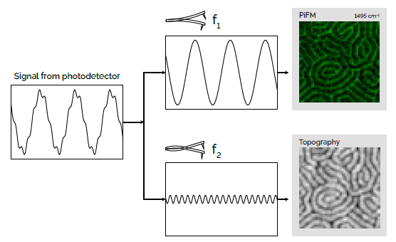
Figure 3. One resonance of the cantilever is used to detect the PiFM signal. Simultaneously, another resonance is used to collect the standard AFM topography and phase in a non-contact manner (no tip/sample contamination). Image Credit: Molecular Vista
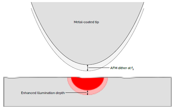
Figure 4. The depth of the tip-enhanced illumination depends heavily on the spacing between the tip and the sample. By detecting the attractive forces in non-contact mode, the measurement is made extremely sensitive – capable of detecting monolayers of material. Image Credit: Molecular Vista
The Result
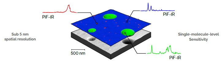
Figure 5. PiF-IR nanoscale spectra are made by measuring the strength of the attractive photo-induced forces as a function of wavenumber. PiFM chemical maps are created by scanning the surface with a fixed-wavenumber to measure absorption strength as a function of position. The color layer over the AFM topography is three fixed-wavenumber PiFM images combined. Image Credit: Molecular Vista
PiFM Chemical Mapping
Reveal Hidden Structure in Color
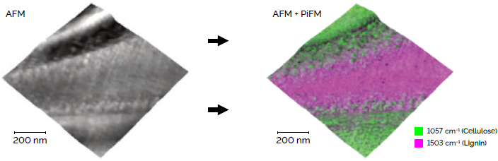
Figure 6. 3D visualization of the AFM topography of a cell wall from an ultra-thin cross-section of spruce wood. An overlay of two PiFM images shows the chemical composition of the surface where lignin and cellulose mix. This PiFM overlay reveals how the materials are distributed, and it shows how some of the topographic features are related to the local chemistry. Scan dimensions: 1 µm × 1 µm × 0.034 µm. Image Credit: Molecular Vista
Sub-5 nm Spatial Resolution
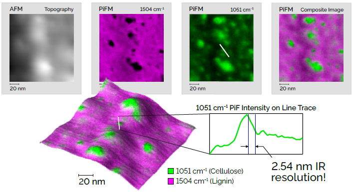
Figure 7. A zoomed-in region of the spruce wood cell wall. At only 150 nm square, this scan area is over 50 times smaller than in Figure 6. PiFM images show the chemical distribution of lignin and cellulose on the surface. A line trace plotting the intensity of the data in the green image shows an IR spatial resolution of less than 5 nm. Notice how the PiFM images bring the topography alive with precise chemical detail while the topography itself is unremarkable. Image Credit: Molecular Vista
Download the Brochure for More Information
PiF-IR Nano-Spectroscopy
Single-Molecule-Level Sensitivity
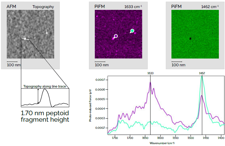
Figure 8. This sample was intended to be a uniform monolayer of peptoid molecules; however, initial PiF-IR analysis indicated that actual peptoid coverage was very sparse. Therefore, a PiFM image was taken at 1633 cm−1 which should highlight any peptoid molecules present. This image reveals tiny peptoid fragments on the surface. A PiF-IR spectrum taken on one of those points shows the characteristic peak at 1633cm−1 despite the peptoid fragment being only 1.7 nm tall! The black spot in the green PiFM image shows that the fragment is sitting on top of the substrate material. Image Credit: Molecular Vista
Excellent Agreement with FTIR
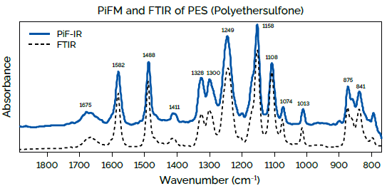
Figure 9. On homogeneous samples, PiF-IR spectra agree with FTIR extremely well. Image Credit: Molecular Vista
Analyze Organic and Inorganic Materials
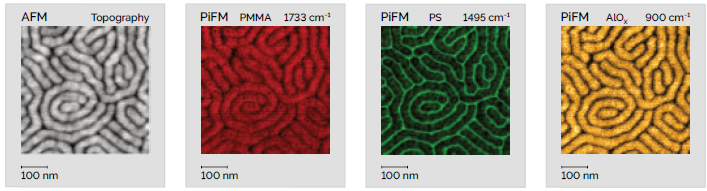
Figure 10. Both organic and inorganic samples can be analyzed equally well using PiFM and PiF-IR. Here, a PS-b-PMMA block copolymer has undergone sequential infiltration synthesis to produce aluminum oxides in the PMMA block. The sample was exposed to a vapor of trimethyl aluminum, which should only react with carbonyl groups in the PMMA. Subsequent exposure to water vapor converts the trimethyl aluminum into aluminum oxide. PiFM analysis after this process confirms the block-selective infiltration by the presence of a new broad peak from 800 to 1100 cm−1 (not shown). A PiFM image taken at 900 cm−1 (yellow image) highlights the infiltrating alumina in the PMMA blocks, demonstrating the exceptional resolution of PiFM chemical mapping even on inorganic samples. Image Credit: Molecular Vista
Orientation Discrimination
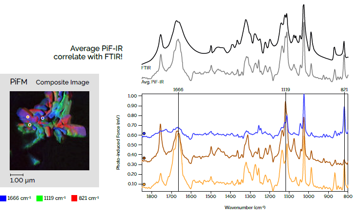
Figure 11. Similar to polarized FTIR, PiF-IR spectra are orientation sensitive due to the tip-enhanced field. The PiF-IR spectra above were acquired at different crystal faces on a vitamin C sample. They exhibit the local IR bands associated with the specific crystal faces. The average of these three distinct local PiF-IR spectra compare nicely with the bulk FTIR spectrum, which is the equivalent of an ensemble average of billions of PiF-IR spectra. Image Credit: Molecular Vista
Download the Brochure for More Information
Comparisons
Comparing Surface Analytical Techniques
Table 1. PiFM & PiF-IR bring molecular analysis to the realm of true nanoscale resolution, providing both IR absorption spectra and chemical mapping with sub-5 nm spatial resolution and monolayer sensitivity, complementing XPS or ToF-SIMS in any high-end lab. *For SEM and TEM, EDS measurements are not as high resolution as is possible for imaging. Source: Molecular Vista
| |
PiFM &
PiF-IR |
Raman |
FTIR |
TOF-
SIMS |
XPS |
TXRF |
SEM/
EDS |
TEM |
Auger |
Species
Detected |
Molecular |
Molecular |
Molecular |
Molecular |
Molecular |
Elemental |
Elemental |
Elemental |
Elemental |
Chemical
Mapping |
Yes |
Yes |
Yes |
Yes |
Yes |
Yes |
Yes |
Yes |
Yes |
Lateral
Resolution |
Sub 5
nm |
> 0.5
μm |
> 10
μm |
100
nm |
Sub 5
μm |
~10
mm |
1 nm
*0.5 μm
EDS |
0.2 nm
*1 – 20 nm
EDS |
8
nm |
Depth
Probed |
20 nm
& bulk |
> 500
nm |
1
μm |
1
nm |
10
nm |
10
nm |
1
μm |
~100
nm |
10
nm |
Vista One Specifications
Source: Molecular Vista
| Stage and scanner |
| Sample stage travel |
75 mm, max sample 140 mm square |
| Scan size |
80 × 80 μm (100 × 100 μm option). |
| Dual Z feedback |
12 μm z-scanner with 600 nm fast z-scanner provides both high bandwidth and a large z-range. |
| Physical requirements |
| Table size |
1.2 m × 1.8 m (4 ft × 6 ft) optical breadboard recommended. |
| Enclosure |
About 13 kg, removable, acoustic insulation, temperature controlled with dry air. |
| Functionality |
| Imaging modes |
nc-AFM, PiFM, KPFM, cAFM, nano DMA, FvD (force vs distance) mapping, Raman, s-SNOM. |
| Spectroscopy modes |
PiF-IR, FvD, Raman. |
| PiF Laser options |
QCL (770 – 1840, 1995 – 2395 cm−1), OPO/DFG (590 – 2050, 2250 – 4400, 5000 – 7000 cm−1). |
| Depth Probed |
20 nm in surface mode & greater than 100 nm in bulk mode. |