Photothermal AFM-IR is a highly effective method for nanoscale chemical analysis, ideally suited to the stringent requirements of semiconductor research and production. By integrating the spatial precision of atomic force microscopy with the chemical specificity offered by infrared (IR) spectroscopy, it facilitates detailed examination of materials and structures at scales below 10 nm.
This article looks at how AFM-IR has been used to tackle key semiconductor development challenges, providing crucial insights into contamination, interfaces, and material properties that are essential for improving device reliability and manufacturing processes.
Photothermal AFM-IR Technology
As device dimensions continue to shrink, the need to detect and chemically identify increasingly smaller contaminants grows critical. Identifying chemical species at submicron and nanoscale dimensions within semiconductor materials presents a significant challenge in both device research and process monitoring or failure analysis settings.
Semiconductor manufacturers employ various analytical methods, including scanning electron microscopy paired with energy dispersive X-ray spectroscopy (SEM/EDX),1 confocal Raman spectroscopy,2 and nanoscale IR (nanoIR) spectroscopy.3 Among these, nanoIR stands out due to its combination of chemical specificity and nanoscale spatial resolution.
NanoIR spectroscopy bridges the gap between conventional IR spectroscopy and atomic force microscopy (AFM). While traditional IR spectroscopy is powerful for chemical identification, its spatial resolution is generally constrained to 3–10 μm by the Abbe diffraction limit.
On the other hand, AFM offers detailed topographical and mechanical property maps but lacks inherent chemical specificity.
Photothermal AFM-IR, often called AFM-IR, is a Bruker-patented nanoIR technique that enables chemical identification with spatial resolution below 10 nm and monolayer-level sensitivity—surpassing the diffraction limit by more than 100-fold. This method is user-friendly and straightforward to interpret.
AFM-IR spectra can be analyzed in a similar manner to Fourier-transform IR spectroscopy (FTIR), utilizing well-established spectral libraries.
During AFM-IR measurements, an infrared laser induces localized thermal expansion in the sample, which in turn applies a mechanical force on the AFM probe. The magnitude of this force is directly proportional to the sample’s IR absorption at the given wavelength, allowing the collection of localized IR spectra.
Since AFM-IR absorption spectra are direct measurements of sample absorption, they correlate closely with conventional bulk IR spectra and are independent of complex optical interactions involving the tip and sample. 4
Nanoscale Contaminant Identification
Photothermal AFM-IR allows for chemical analysis of nanocontaminants at very high resolution, a capability crucial for applications involving both wafers and photomasks.
Typically, TappingMode AFM is first utilized to detect contaminants, followed by IR absorption mapping at a fixed wavenumber and point spectroscopy to determine their chemical composition.
To illustrate nanoscale chemical characterization, samples were prepared using known materials commonly found in semiconductor fabrication environments, including a polymer nanocontaminant (2 nm in height and approximately 35 nm in diameter), shown in the high-resolution AFM topography overview scan in Figure 1a.
Once the contaminant was identified in the review scan, a higher resolution AFM-IR scan was performed at 1760 cm-1 to generate a chemical map (Figure 1b).
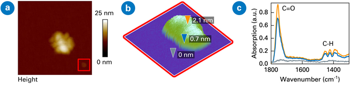
Figure 1. (a) Topography with scan size 500x500 nm and (b) IR map of 100x100 nm on a selected nanocontaminant (2 nm height, 35 nm diameter), and IR spectra on substrate and nanocontaminant. Sample courtesy of EAG Laboratories. Image Credit: Bruker Nano Surfaces and Metrology
AFM-IR spectra were then collected from three locations indicated in Figure 1c: on the substrate (gray), on top of the contaminant (orange), and near the contaminant’s edge (blue).
The spectra recorded atop and at the edge of the contaminant revealed characteristic functional groups (e.g., C=O and C-H) absent in the substrate spectrum. This outcome demonstrates photothermal AFM-IR’s capability for chemical identification and mapping of nanocontaminants.
KLARF-Based Navigation
KLARF coordinate file–based navigation allows for precise targeting of known contamination sites, improving both detection and redetection efficiency. By incorporating KLARF navigation, the photothermal AFM-IR workflow becomes more streamlined, enabling faster identification and mapping of nanoscale contaminants.
In the example shown in Figure 2, KLARF navigation directed the AFM-IR system to a cluster of nanocontaminants ranging from 50 to 200 nm in size.
While topographic AFM imaging alone could not differentiate contaminant types, IR maps collected at multiple wavenumbers revealed five distinct chemical functionalities.
A composite image of the IR absorption maps at these wavenumbers highlights contaminant distribution (Figure 2b), while spectra acquired from each type allowed clear chemical differentiation (Figure 2c).
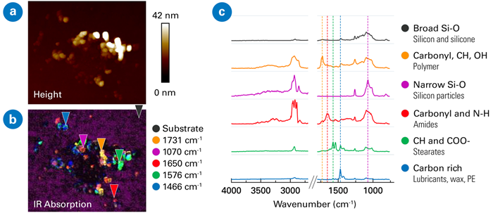
Figure 2. (a) Topography (2x2 μm scan) and (b) composite IR map combining IR absorption at different wavenumbers corresponding to five different materials showing contaminant distribution, and (c) corresponding AFM-IR spectra in selected contaminants. Image Credit: Bruker Nano Surfaces and Metrology
Dielectrics
Photothermal AFM-IR complements other dielectric characterization methods, contributing to a more comprehensive understanding of structure-property relationships. This enriched insight into dielectric behavior supports improved performance across applications such as microelectronics, capacitors, and insulating materials. 5
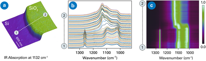
Figure 3. (a) Tapping AFM-IR data on Si/SiO2 interface (scan size 1x1 μm) and (b) IR spectra along a line (660 nm length) crossing the interface with (c) corresponding color map. Image Credit: Bruker Nano Surfaces and Metrology
AFM-IR is used to identify functional groups, detect impurities, and uncover structural disorder in dielectrics by linking specific vibrational frequencies to dielectric properties like permittivity and loss factor.
Figure 3a shows an AFM-IR absorption map collected at 1132 cm-1 at a Si/SiO2 interface, where strong absorption corresponds to the Si–O–Si bonding region in SiO2.
Spectra taken along a line across this interface (Figure 3b) display peak shifts between 1125 and 1134 cm-1, reflecting variations in crystallinity or structure near the step edge. Color maps visualizing IR absorption as a function of location and wavenumber (Figure 3c) provide an integrated view of chemical and structural changes across the interface.
Thin Films and Coatings
Thin films and coatings play a vital role in enhancing the performance and durability of modern semiconductor devices, with some coatings as thin as monolayers. These films serve various purposes, including protection, adhesion modification, and functional layers in lithography, etching, and dielectric patterning.
Photothermal AFM-IR uniquely enables chemical characterization of these films on the nanoscale, even for monolayer coatings such as self-assembled monolayers (SAMs). SAMs protect surfaces from environmental factors like static and adhesion forces and act as a protective layer to reduce device wear.
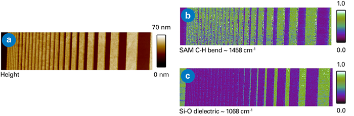
Figure 4. (a) Topography and (b/c) IR absorption maps of dense line-space structures with SAM on top of the lines and dielectric in the trenches. Scan size (horizontal) 10 μm. Image Credit: Bruker Nano Surfaces and Metrology
Figure 4 presents AFM-IR data of a selectively applied SAM coating on dense line/space structures.
Imaging at 1458 cm-1 (Figure 4b) showed strong absorption corresponding to the C–H bend in the SAM, while imaging at 1068 cm-1 (Figure 4c) highlighted absorption related to the Si–O dielectric. These IR maps collected at specific wavenumbers clearly differentiate between SAM-coated areas and exposed dielectric surfaces, even across this complex geometry.
Photoresist Film Analysis
Photoresists play a central role in semiconductor lithography, defining patterns on silicon wafers during device fabrication. As device geometries continue to shrink and process complexity grows, understanding the chemical and structural behavior of photoresist films is increasingly important for improving pattern fidelity and reducing defects.
Photothermal AFM-IR provides high-resolution chemical mapping of photoresist films, revealing nanoscale variations in functional groups and molecular structure. This capability is especially valuable for assessing how photoresists respond to exposure and processing, and how these changes ultimately affect pattern formation and resolution.
By pinpointing localized chemical modifications, AFM-IR supports the optimization of lithographic processes and the design of next-generation photoresists, including metal oxide, chemically amplified, and molecular resists.
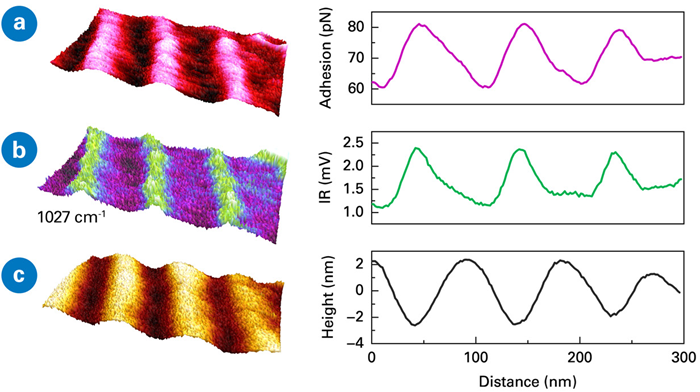
Figure 5. Resonance Enhanced Force Volume (REFV) AFM-IR data for (a) adhesion, (b) IR absorption, and (c) topography on a 35 nm thick photoresist exposed to a 50 mJ dose (325x159 nm scan). Sample courtesy: TNO Delft (NL) and University of Amsterdam (NL). Image Credit: Bruker Nano Surfaces and Metrology
Co-localized data combining chemical and mechanical properties is especially useful for photoresist characterization. The Resonance Enhanced Force Volume (REFV) AFM-IR mode provides artifact-free, co-localized maps of mechanical and IR absorption properties.6
In Figure 5, REFV AFM-IR mapped adhesion, IR absorbance, and height across a 35 nm thick photoresist film exposed to a 50 mJ dose. The results showed higher IR absorbance in valleys compared to ridges, demonstrating nanoscale spatial resolution at around 10 nm.
Patterned Structures
Patterned semiconductor features pose unique challenges for chemical characterization due to their intricate geometries and submicron sizes. Photothermal AFM-IR excels by delivering localized chemical data with exceptional spatial resolution.
For instance, in low-k α-SiOC:H/Cu interconnects, AFM-IR differentiates chemically distinct areas within dielectric layers even when features are below the spatial resolution limits of conventional IR spectroscopy. 7
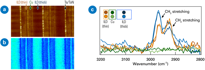
Figure 6. (a) Topography and (b) IR absorption map at 2960 cm-1 on patterned Cu/dielectric interconnect sample (10x5 μm scan). Spectra in selected positions show differences in C-H stretching (marker color corresponds to that of individual spectra). Image Credit: Bruker Nano Surfaces and Metrology
Figure 6 illustrates the interconnect structure from Reference 7, showing alternating copper (Cu) and SiOC:H interlayer dielectric (ILD) layers with low-k α-SiOC:H widths ranging from 1650 nm to 330 nm.
IR spectra collected from marked locations (Figure 6a) on both Cu and exposed α-SiOC:H dielectric regions revealed clear differences in the C–H spectral region between narrow and wide dielectric areas.
The reduced intensity of the CH3 mode in narrower α-SiOC:H regions aligns with the modification or loss of terminal CH3 groups caused by plasma etching and ashing processes used for dielectric patterning.
AFM-IR Brings Nanoscale Chemical Analysis to Semiconductor Applications
Photothermal AFM-IR provides a powerful approach for nanoscale chemical analysis in semiconductor research and manufacturing. By combining the spatial resolution of atomic force microscopy with the chemical specificity of IR spectroscopy, it enables direct, localized characterization of nanocontaminants, dielectrics, photoresists, thin films, and coatings.
Offering chemical insights at the sub-10 nm scale—beyond the reach of conventional techniques—AFM-IR supports process optimization, materials development, and failure analysis.
Acknowledgments
This article is based on materials originally authored by Cassandra Phillips, Ph.D., Chunzeng Li, Ph.D., Erica Erickson, Ph.D., Jinhee Kim, Ph.D., Peter De Wolf, Ph.D., and Qichi Hu, Ph.D., researchers at Bruker Corporation.
References
- Goldstein, J.I., et al. (2018). Scanning Electron Microscopy and X-Ray Microanalysis. (online) New York, NY: Springer New York. https://doi.org/10.1007/978-1-4939-6676-9.
- Chen, W.-L., et al. (2013). Depth-resolved confocal micro-Raman spectroscopy for characterizing GaN-based light emitting diode structures. Review of Scientific Instruments, (online) 84(11), p.113108. https://doi.org/10.1063/1.4829627.
- Mathurin, J., et al. (2022). Photothermal AFM-IR spectroscopy and imaging: Status, challenges, and trends. Journal of Applied Physics, 131(1), p.010901. https://doi.org/10.1063/5.0063902.
- Dazzi, A., et al. (2005). Local infrared microspectroscopy with subwavelength spatial resolution with an atomic force microscope tip used as a photothermal sensor. Optics Letters, 30(18), p.2388. https://doi.org/10.1364/ol.30.002388.
- Sayan, S., et al. (2005). Structural, electronic, and dielectric properties of ultrathin zirconia films on silicon. Applied Physics Letters, (online) 86(15). https://doi.org/10.1063/1.1864235.
- Bruker. (2022). Resonance Enhanced Force Volume AFM-IR (REFV AFM-IR). (online) Available at: https://www.bruker.com/en/products-and-solutions/infrared-and-raman/nanoscale-infrared-spectrometers/resource-library/an-207-resonance-enhanced-force-volume-afm-ir-refv-afm-ir.html (Accessed 10 Sep. 2025).
- Michael, Alexandre Dazzi, Marcott, C.A., Dillon, E. and King, S.W. (2015). Nanoscale Chemical-Mechanical Characterization of Nanoelectronic Low- k Dielectric/Cu Interconnects. ECS Journal of Solid State Science and Technology, (online) 5(4), pp.P3018–P3024. https://doi.org/10.1149/2.0041604jss.

This information has been sourced, reviewed and adapted from materials provided by Bruker Nano Surfaces and Metrology.
For more information on this source, please visit Bruker Nano Surfaces and Metrology.