Sponsored by MKS NewportReviewed by Olivia FrostJul 8 2026
Hybrid bonding has the potential to significantly advance semiconductor packaging by enabling smaller, more compact assemblies that deliver higher performance and greater reliability.

Image Credit: asharkyu/Shutterstock.com
Hybrid bonding and similar technologies will grow in importance as more advanced 3D packaging techniques are increasingly adopted and interconnection pitches shrink below 10 μm, with the current roadmap already pointing towards submicron. This technology will be key for enabling high bandwidth memory (HBM), 3D NAND, and high-performance computing 3D system on chip (HPC 3D SoC).
Precise and stable motion and positioning are crucial parameters in hybrid bonding systems. This is necessary to ensure accurate alignment, which is fundamental for effective hybrid bonding.
MKS excels in this domain, drawing on more than six decades of experience to deliver advanced motion and positioning solutions for hybrid bonding tool builders.
The company’s technologies support all integration levels, from components to turnkey subsystems, fueling innovation and enhancing semiconductor production capabilities.
The following sections detail the specific requirements of hybrid bonding, as well as the ways that MKS can support system developers with motion platforms.
Key Hybrid Bonding Benefits
The necessity for hybrid bonding is relatively easy to understand: to achieve greater miniaturization in microelectronic devices, chips must be assembled into stacks with increased packing density.
Moreover, these stacked chips themselves must shrink, in part by using more closely spaced (finer pitch) interconnects. Even the height (thickness) of these interconnects must be minimized to reduce total stack thickness.
Hybrid bonding shows the most promise for assembling these smaller, finer-pitched dies. It provides multiple advantages over conventional bonding techniques such as wire bonding, flip-chip, and thermo-compression bonding (TCB). These benefits include:
- High Density and Fine Pitch: Hybrid bonding is frequently under 10 μm, compared to the larger pitches required by wire bonding and flip-chip techniques, and the standoff distance between each die is reduced to virtually zero.
- Low Power Consumption: Shorter interconnects minimize parasitic capacitance and resistance, resulting in reduced power consumption.
- Enhanced Thermal and Electrical Performance: Direct metal-to-metal connections deliver exceptional thermal conductivity and enhanced heat dissipation. Electrical performance is improved by minimizing inductance and resistance, resulting in faster signal transmission and reduced signal loss.
- Improved Dependability: Durable mechanical bonds, with high resistance to thermal and mechanical stress, provide long-term stability.
- Scalability: Hybrid bonding is scalable to future technology nodes, supporting the ongoing push towards smaller, more robust semiconductor devices. Due to its compatibility with diverse materials and procedures, it is adaptable for future developments in semiconductor production.
Hybrid Bonding Basics
Hybrid bonding involves bringing two flat, smooth, and clean surfaces of similar materials into contact. This forms powerful interatomic bonds between the two surfaces without requiring adhesives or solders. The actual bonding mechanism varies according to the substance.
Specifically, direct bonding of two dielectric (SiO2) surfaces yields covalent bonds, whereas direct bonding of two copper (Cu) surfaces produces a metallurgical bond during a two-step annealing procedure.

Key process steps of hybrid bonding. Image Credit: MKS Newport
The graphic illustrates the main stages in the hybrid bonding procedure. These are:
- A hybrid bond layer is produced on top of a finished wafer (a wafer where all front-end-of-line and back-end-of-line processes are complete). The hybrid bond layer consists of a dielectric, typically SiO2, and copper pads.
- Cleaning and chemical mechanical polishing (CMP) make the surface of the bond layer exceptionally smooth and flat. The copper is “dished,” or made slightly concave, because it expands more than the dielectric during annealing. For this reason, a small gap is necessary to accommodate this differential expansion.
- Plasma activation then modifies the bond layer's surface characteristics, improving its capacity to bond with other materials.
- The wafer or dies to be bonded are accurately aligned to the original wafer. The surface(s) of all these have been prepared using the same method as described.
- The components are all brought into contact, and the actual bonding of the dielectric material is initiated. This is achieved at room temperature.
- Annealing is subsequently carried out under pressure and at a high temperature. This process typically involves two phases. First, a lower-temperature annealing step finalizes the dielectric bonding. Following this, the copper expands to completely fill the small remaining gaps and create direct bonds.
There is a wide variety of specific embodiments of hybrid bonding. Moreover, the procedure can be conducted wafer-to-wafer (W2W), die-to-wafer (D2W), or die-to-die (D2D).
Each of these techniques has its own benefits and drawbacks regarding throughput, yield, and cost, and therefore has specific applications for which it is most useful.
Motion Requirements
Most stages of the hybrid bonding procedure are challenging. Specifically, the process demands exceptionally flat and clean surfaces, which must be positioned and held relative to each other with high precision and repeatability. Consequently, the mechanical tolerances become progressively tighter as die geometries and pitch dimensions shrink.
The specific requirements of the motion system vary based on the exact implementation. However, broad generalizations can be made regarding hybrid bonding for W2W and D2W, which serve to illustrate the core differences between these applications.
The motion system parameters of greatest relevance are generally alignment, stability, and repeatability. Since hybrid bonding critically depends on surface cleanliness, the system must completely eliminate the risk of introducing contamination.
Furthermore, throughput, which ultimately dictates cost, remains a constant consideration for semiconductor capital equipment.
Alignment
First, the motion system must move the two surfaces (two wafers or a die and a wafer) with high precision, repeatability, and control to achieve the desired alignment and positioning. This procedure is most often supported with a vision system (operating in either the visible or infrared), which identifies fiducial marks on the components.
Alignment for W2W bonding is generally more challenging than D2W. For W2W, overall alignment accuracy often lies in the hundreds of nanometers or less range. However, for wafers, this accuracy only needs to be maintained over a range of tens of centimeters.
For hybrid bonding, placement precision depends on pad size. A 500 nm alignment accuracy is typically a minimum requirement, extending down into the 100–200 nm range for some applications.
The movement range can span hundreds of centimeters, depending on whether the motion system is conducting pick-and-place operations for D2W or if off-axis alignment is needed for W2W. If through-silicon alignment (TSA) using IR is possible, then the XY motion is minimal (under a centimeter).
After the fiducial locations for both pieces are found, the wafer/die is moved in XY to the approximate location prior to making the final fine alignment, and the surfaces are precisely brought together in Z for bonding.
Various techniques (such as edge-first or center-first) are employed to control the bond front propagation, eliminating the risk of air pockets interfering with the bonding operation.
Repeatability
Repeatability serves as the primary specification of the motion system. High repeatability guarantees that variations in the mechanical components or vision system will not substantially impact the final alignment result across different bonding cycles.
Motion system performance is the key deciding factor in repeatability, though it can also be affected by variations in camera resolution, lighting conditions, and calibration, or external factors such as room temperature, humidity, or vibration.
Stability
Stability is another crucial factor, particularly throughout the bonding process and during inspection stages. Given that this cycle may last several seconds, it can be difficult to maintain stability during bonding.
Moreover, vibration damping and active vibration isolation are needed to mitigate the impacts of both internal and external perturbation sources. Generally, positional stability must be maintained within a fraction of the specified alignment tolerance during the bonding procedure.
MKS' Solutions
As shown, many parameters should be considered when designing a motion platform for hybrid bonding.
Successful navigation of these obstacles requires specialized skill and customized solutions. There are no “off-the-shelf” answers when it comes to achieving maximum levels of performance, efficiency, and dependability. Providing these client-specific solutions is where MKS excels.
First, the company can integrate and tailor systems based on an in-depth understanding of client requirements. Next, it has a large and diverse set of motion-control products and technologies related to hybrid bonding that enable and enhance this capability. These include:
- Air bearings, such as the technology to ensure Z axial rigidity and stability during bonding
- Complex parallel robots for six-degree-of-freedom wafer positioning
- The capacity to use ceramics for high-stiffness, multi-axis monolithic structures
- Cutting-edge rails systems
- High precision and repeatability phases for camera positioning
- Metrology capabilities necessary for validating performance
- Thermal simulation and management for long-term repeatability
- Passive and active isolation integration
- High power and accurate motion electronics for dynamic positioning
- Simulation and prototyping software to optimize and speed up time to market
- The ability to provide a solution to client-specific problems and optimize the criteria that matter most to them
Building on this, MKS delivers integrated, advanced motion platforms for OEMs that feature miniaturized, lightweight designs with high dynamic abilities that ensure superior performance in harsh settings such as cleanrooms.
In addition, the company has significant experience in semiconductor production, including the submicron precision systems used in inspection, metrology, lithography, and other semiconductor applications.
MKS has already participated in the development of both W2W and D2W bonding alignment platforms and related inspection systems, proving its capacity to manage the intricate challenges of hybrid bonding. Examples of a full motion system and specific subsystems the company has engineered for hybrid bonding applications include:
- A fully integrated hybrid bonding motion module
- A parallel robot of W2W hybrid bonding
- A monolithic chuck holder
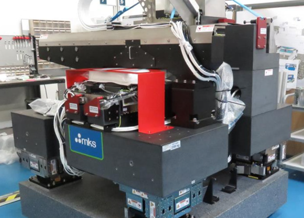
Fully integrated hybrid bonding motion module. Image Credit: MKS Newport
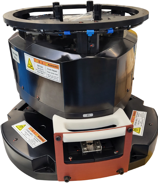
Parallel Robot for W2W Hybrid Bonding. Image Credit: MKS Newport
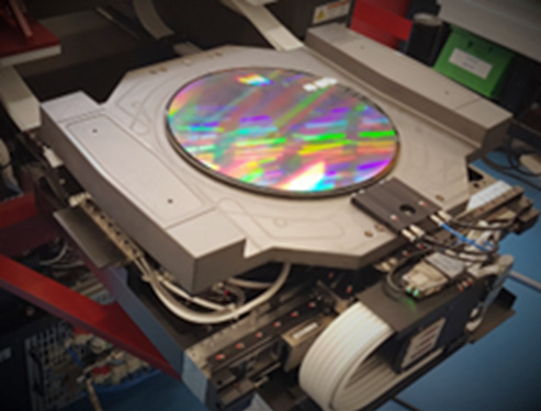
Monolithic chuck holder. Image Credit: MKS Newport
The global reach of MKS ensures quick and effective support from the initial consultation phase through ongoing service for installed systems. The company has facilities and expert teams in the United States, France, Korea, China, and Taiwan to deliver in-depth service and support for its motion control solutions.
In addition, MKS' vertically integrated production footprint, including ISO 6 and ISO 7 cleanrooms, guarantees high-quality standards and the efficient delivery of complex motion systems.
Conclusion
With broad expertise and far-reaching capabilities, MKS helps clients optimize performance, reduce expenses, and mitigate risks in the development of hybrid bonding systems. The company is also committed to forming lasting partnerships with clients.
MKS recognizes that the semiconductor sector is dynamic and requires constant innovation. Through close collaboration with customers, the company ensures its technology roadmap aligns with customers’ requirements, helping it stay ahead of technological demands and the competition.

This information has been sourced, reviewed, and adapted from materials provided by MKS Newport.
For more information on this source, please visit MKS Newport.