The multi-mode gas cluster ion source (GCIS) is designed to operate in both Arn+ cluster and Ar+ monatomic modes, making it suitable for sputter cleaning and depth profiling organic, inorganic and metallic thin films. As well as this, it can also generate low energy He+ ions to use in ion scattering spectroscopy. It is now widely accepted to use large argon clusters for sputter depth profiling of organic materials and that use is being expanded to inorganic depth profiling. A wide range of materials may be sputter cleaned or depth profiled without chemical damage of the surface using a combination of cluster size and acceleration voltage. The ion source can be used in monatomic mode for thin metal layers, small clusters at high beam energies may be used for metal oxides and large clusters at low or medium energy for a wide range of organic materials.
Novel approaches in depth profiling of organic materials are based on sputtering with large Arn+ ion clusters. These clusters can consist of hundreds or even thousands of Ar atoms. As opposed to monatomic ions, large cluster ions will not penetrate deeply into the material therefore the energy of the impact is deposited within the first few nanometers of the surface. As the energy is divided amongst all atoms in the cluster, the energy per projectile atom, or partition energy, can be as low as a few electron volts such that the cluster ions only sputter material from the near-surface region leaving the subsurface layer undisturbed.
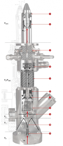
Arn+ Gas Cluster Operating Mode
Large Ar clusters are formed by isentropic adiabatic cooling of the gas as it expands from high pressure (P0) via a nozzle into the vacuum of the source region (P1 / P2). The Arn clusters are ionized by electron impact, extracted from the source region and accelerated along the ion column where a Wien velocity filter is used to select a median cluster size between 500 and 3000. These cluster ions may be accelerated up to a maximum of 20 keV such that the energy per atom, or partition energy, can be varied from <2 eV (5 keV, Ar3000+) to 40 eV (20 keV, Ar500+ ). An ion channeling bend in the focusing column then removes energetic neutrals.
The beam is then focused to a minimum spot size of 250 μm on the sample. Scan plates allow the beam to be rastered across the surface of the sample to produce an even sputter crater. The ability to generate Arn+ ions with different cluster sizes and acceleration energies means successful depth profiles can be generated from the widest range of materials. Large clusters, where n > 2000, are useful for depth profiling organic layer systems whilst smaller, high energy, clusters of n=500 have been shown to be necessary in retaining chemistry of inorganic materials during depth profiling and sample cleaning.
Ar+ Monatomic Operating Mode
The ion source can be operated in monatomic Ar+ ion mode for conventional depth profiling inorganic and metallic samples. This yields a much higher sputter in this class of materials, which is known to be much higher for monatomic than cluster ions, making Ar+ monatomic mode key for depth profiling in realistic experimental times. Ion acceleration voltage can be varied between 500 eV and 8 keV.
Applications
Inorganic Depth Profiling
Small Cluster, High Energy Depth Profiling
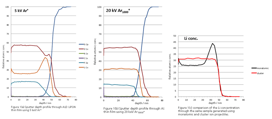
It is known that the sputter yields from inorganic materials are low when using gas clusters. This difficulty can be mitigated by using small clusters with high beam energy. Here we contrast the use of 5 keV monatomic Ar+ with 20 keV Ar1000+ ions for sputter depth profiling a lithium phosphorous oxynitride ALD thin film where the Li distribution through the film is of interest. To ensure the depth profile is completed in reasonable time the high acceleration voltage can be used in cluster mode. There is a distinct difference between the two profiles. Under monatomic bombardment there is an initial increase in Li concentration after the first etch cycle – a result of removing surface contamination – then a subsequent reduction in Li into the bulk of the film reaching a steady-state, shown in figure 1(a). Near the LiPON interface with Si substrate the Li concentration increases.
By contrast when profiled 20 kV Ar1000+ ions the profile shows a different distribution of Li, figure 1(b). At first an increase in Li concentration is shown after the first etch however there is no accompanying decrease. Interestingly no accumulation of Li was seen at the interface with the Si substrate. A comparison of the Li concentrations profiled using two different ions is shown in figure 1(c). The different results are attributed to positive charge build-up in the near surface region from implanted monatomic Ar+ ions.
Charge build-up repels the small, mobile positive Li ions in the surface further into the bulk resulting in an underestimation in surface quantification. Repulsive bulk migration also accounts for the increase in Li concentration at the interface with the Si substrate. The light ions are unable to penetrate into the Si metal and native oxide and instead accumulate at the interface.
Nanostructured Multilayer Materials
Large Cluster, High Energy Depth Profiling
Nanostructured multilayer materials have recently been used as coatings for cutting tools and turbine coatings due to being their classification as super-hard materials. Physical vapor deposition (PVD) is used to assemble nanometer repeating layers into superlattices. An example of such a material is TiN (7 nm)/CrN (3 nm) multilayer with 100 repeat units which has demonstrates high resistance to oxidation and superior mechanical properties.
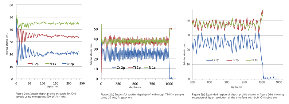
The conventional approach to depth profiling this sample would be to use 500 eV monatomic Ar+ ions. The profile is shown in figure 2(a). The first thing noticed is that there is a loss of interface resolution after 6 repeat units (12 layers) due to penetration of the monatomic Ar+ions into the material resulting in mixing of the layers. This was supported by the observation of Ar in the photoemission survey spectrum during the depth profile.
The same sample was profiled using high energy, large clusters (20 keV, Ar2000+). The use of the high ion acceleration voltage made sure that the yield volume per incident ion was as high as possible so that the depth profile was completed in an overnight experiment with a sputter rate of a few nm / minute.
Figure 2(b) shows the successful depth profile with retention of the layer structure throughout the 100 layer coating. In contrast to the monatomic profile Ar incorporation into the sample was not observed for this Ar2000+ cluster profile.
Organic Multilayer Depth Profile
Small Cluster, Medium Energy Depth Profiling
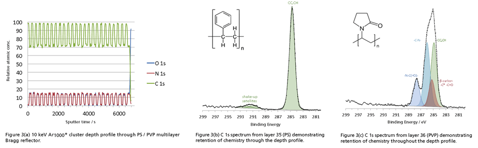
Thin film polymer structures are increasingly being used in a variety of areas including optical filters and reflectors, organic electronics and drug delivery systems. The use of gas clusters means these materials can be analyzed through sputter depth profiling, and the chemistry of the polymer remains unchanged. Here, 10 keV Ar1000+ ions were used to depth profile through a 50 layer multilayer Bragg reflector comprising spin-coated polystyrene (PS) and polyvinylpyrrolidone (PVP). The PS & PVP layers were 328 nm and 288 nm respectively such that the complete structure was >15 um thick. Figure 3(a) shows the sputter depth profile through the entire structure to the glass substrate. The layer structure is retained throughout the depth profile and it is evident that the fabrication of the structure resulted in uniform layer thickness for each respective polymer layer. Figures 3(b) and (c) show the C 1s spectrum for layers 35 and 36 respectively, proving the chemistry of the polymer is retained during the sputtering process.
Maximum Flexibility
Published work1 has shown that different types of polymer can vary in sputter yields, which depends on the size and energy of the cluster. To achieve maximum flexibility in terms of the range of materials which can be successfully profiled, the ion source parameters, including cluster size and primary beam energy, can be defined specifically to optimize sputter yield of the specimen under investigation. Poly (lactic-co-glycolic) PLGA acid is a well known Type II polymer[2]. Data acquired using the GCIS Arn+ [Figure 4] shows that the sputter yield of PLGA is highly dependent upon the primary beam energy. As well as this it is clear that the capability to generate ions with 20 keV energy results in greater ion yield for PLGA.
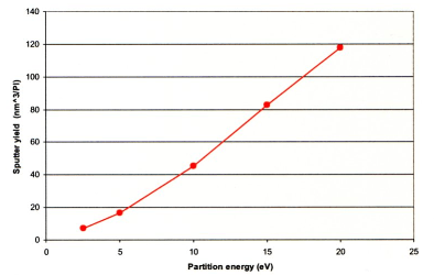
Figure 4. Sputter yields for Ar1000+ at a range of primary beam energies on 60 nm thin film PLGA polymer on Si
Organic/Organic Multilayer Depth Profile (Ar500+)
The following example is a sputter depth profile through an organic/organic multilayer sample with 10 alternating layers of a polyester with high nitrogen concentration and a methylmethacrylate with low nitrogen concentration where each polymer layer is nominally 100 nm thick. The sample is shown as a schematic diagram in Figure 5.
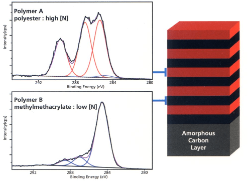
Figure 5. Polymer / polymer multilayer and representative spectra from each layer
A 110 µm area centered in a 1.5 x 1.5 mm2 sputter crater was analyzed for data. The GCIS was used in cluster mode with Ar500+ accelerated to 5 keV, which gave a partition energy of 10 eV per atom. The concentration depth profile is shown in Figure 6 with the carbon chemical state plotted against sputter depth. It is immediately apparent that the sputter yield for both polymers is extremely close under the ion source parameters used giving an average etch rate of 18.5 nm/min for the bilayers. It is further noted that excellent interface resolution is kept throughout the profile with the interface resolution between polymer layers 9 and 10 measured as 15 nm. Figure 7 shows the narrow region scans for C 1s, 0 1s and N 1s as a function of sputter cycle. This demonstrates that the chemistry of both polymers is retained throughout the depth profile.
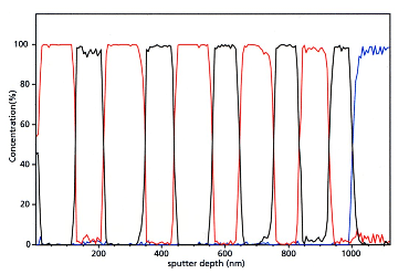
Figure 6. C 1s chemical state depth profile for polymer/polymer multilayer
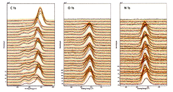
Figure 7. High resolution, narrow region scans for C Is, 0 1s and N 1s regions as a function of sputter cycle. The 'as introduced' surface is at the bottom of the figure with increasing etch time vertically to the bulk amorphous carbon substrate at the top of each plot