Nov 20 2013
EV Group (EVG), a leading supplier of wafer bonding and lithography equipment for the MEMS, nanotechnology and semiconductor markets, today introduced the EVG®PHABLE™ exposure system, which is designed specifically for manufacturing photonic components.
Leveraging EVG's expertise in photolithography, the EVG PHABLE system incorporates a unique contactless lithography mask-based approach that enables full-field, high-resolution and cost-efficient micro- and nanopatterning of passive and active photonic components, such as patterned structures on light emitting diode (LED) wafers, in high-throughput production environments.
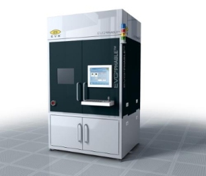 The EVG(r)PHABLE(tm) from EV Group is a non-contact mask-based lithography solution that enables full-field, high-resolution and cost-efficient micro- and nanopatterning of passive and active photonic components, such as patterned structures on light emitting diode (LED) wafers, in high-throughput production environments. (PRNewsFoto/EV Group)
The EVG PHABLE exposure system is the first fully-automated production equipment to feature PHABLE™ ("photonics enabler") technology from Eulitha AG, a pioneer in lithography tools based in Villigen PSI, Switzerland. Integrating Eulitha's full-field exposure technology with EVG's well-established nanolithography production platform provides a unique solution for the automated fabrication of photonic nanostructures.
The EVG PHABLE system combines the low cost-of-ownership, ease-of-use and non-contact capabilities of proximity lithography with the sub-micron resolution of lithography steppers to provide low-cost automated fabrication of photonic patterns over large areas. This makes it ideally suited for patterned sapphire substrates (PSS) or to enhance the light extraction (and thus the efficiency) of LED devices. The EVG PHABLE system includes a unique Displacement Talbot Lithography approach that enables it to produce features ranging from three microns down to 200 nm with effectively no depth-of-focus limitation or stitching effects that can arise from using steppers on substrates with rather poor total thickness variation. As a result, it can be used to pattern substrates up to six inches in diameter in a single exposure step. This approach also enables the EVG PHABLE system to maintain consistently high patterning throughput independent of the size of the processed wafer, as well as maintain very large exposure gaps (up to several hundreds of microns) between the mask and wafer, thereby avoiding process-related mask contamination.
"We are excited to enter the commercialization phase of our collaboration with Eulitha," stated Hermann Waltl, executive sales and customer support director at EV Group. "The EVG PHABLE system broadens EVG's micro- and nanopatterning process portfolio, providing a unique, very cost-efficient solution to our customers in the LED, optics and photonics markets. The novel equipment clearly demonstrates the synergies of our respective technologies."
The EVG PHABLE system can produce both one-dimensional patterns, such as lines and spaces, as well as two-dimensional patterns, such as hexagonal or square lattices. Thus, it supports a variety of approaches to enhance the light extraction from LEDs. These include LED surface structuring, PSS, photonic crystal applications, nano-wire LEDs and optical gratings. The system can also be configured for photovoltaic, optics or biomedical manufacturing applications.
About Eulitha
Eulitha AG is a spin-off company of the Paul Scherrer Institute, Switzerland. It specializes in the development of innovative lithographic technologies for applications in optoelectronics, photonics, biotechnology, and data storage. It produces and markets nano-patterned wafers and templates using its unique EUV interference method and state-of-the-art e-beam lithography tools. PHABLE is the brand name of its new photolithography platform, which includes exposure tools and wafer patterning services. For more information about Eulitha, please visit www.eulitha.com.
About EV Group (EVG)
EV Group (EVG) is a leading supplier of equipment and process solutions for the manufacture of semiconductors, microelectromechanical systems (MEMS), compound semiconductors, power devices and nanotechnology devices. Key products include wafer bonding, thin-wafer processing, lithography/nanoimprint lithography (NIL) and metrology equipment, as well as photoresist coaters, cleaners and inspection systems. Founded in 1980, EV Group services and supports an elaborate network of global customers and partners all over the world.