Maintaining wafer geometry is critical to semiconductor processes involving precision handling, inspection, metrology, and bonding. At SEMICON West 2026, Physik Instrumente (PI) introduced an active wafer chuck that uses piezo-based actuation to actively manipulate wafer shape, enabling compensation for deformation that can interfere with positioning and process accuracy.
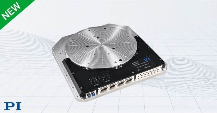 PI introduced the piezo-driven active wafer chuck at SEMICON West, 2026. Image Credit: PI (Physik Instrumente) LP
The system supports shaping based on the first ten Zernike modes as well as freely selectable deformation patterns. This enables engineers to tailor correction to specific wafer geometries and application requirements. With support for substrates up to 300 mm, the technology provides a flexible platform for integration into advanced semiconductor equipment.
PI's active wafer-shaping technology brings precision actuation to wafer-level surface control, helping equipment developers address demanding requirements for substrate flatness and positioning.
Applications and Industries Served
Semiconductor manufacturing, wafer warpage correction, active surface shaping, advanced packaging, wafer inspection & metrology, wafer handling & processing, precision metrology.