|
Carbon nanotubes have been shown to posses a number of remarkable properties(1-4). It has previously been shown that carbon nanotubes can be grown by Chemical Vapour Deposition (CVD) in such a way as to span gaps between catalyst particles(5,6). The growth of junction nanotubes(5,7-12) offers many exciting possibilities for electrical device applications including the introduction of carbon nanotubes into integrated circuit chip design(13-16). Though many of these applications require the use of single wall nanotubes (SWNT) the study of MWNT junctions is still useful both for applications directly requiring MWNTs for their metallic electrical behaviour such as interconnects and as a precursor for SWNT research. Though junction structure nanotubes have been made by other methods(17,18) CVD allows in situ patterning of these structures Here we present a simple method of growing controllable densities of interconnect type MWNTs with high proportions of Y-junction and multiple junction nanotubes across etched patterns, using a simple catalyst preparation.
Experimental
The MWNTs were grown in a custom built CVD system based on a single-stage Linberg blue mini-mite horizontal tube furnace fitted with an 18mm inner diameter alumina furnace tube. The active gas used was acetylene, C2H2, with flow rates between 0.05 – 1 slm used, argon was used as the carrier gas with a flow ratio of 10:1 Ar: C2H2. Both gas flow rates were controlled using mass flow controllers. The active gas was flowed through the system in the temperature regime of 700 – 900°C for between 40 – 120 minutes. The temperature was kept stable while the active gas was flowing. The substrates used were 10mm * 10mm Si/SiO2 wafer segments with a “test card” array of patterns etched into the surface. Each test segment used was selected to have at least one etched pattern of interest with each pattern covering an area of approximately 100 µm2. The patterns used were all trench structures with widths ranging from 200 – 1000 nm, trench separations were of the order of 200 – 500 nm and trench depths of 300 – 400 nm. The catalyst used was a solution of a block co-polymer polystyrene-polyvinylferrocene (PS-PVP) in toluene that was simply drop-cast onto the substrate surface and the solvent allowed to evaporate off at room temperature. The PS-PVP was anionically synthesized in house(19), and characterized by Nuclear Magnetic Resonance and Gel Permeation Chromatography (not shown) to determine its iron content (2.1%).
Scanning Electron Microscopy
Scanning Electron Microscopy (SEM) was carried out on a Hitachi S-4300 Field Emission SEM. Samples were coated with a 5nm layer of gold prior to SEM analysis to prevent surface charging effects.
Transmission Electron Microscopy
Low resolution Transmission Electron Microscopy was carried out on a Hitachi H-7000 TEM. Raman studies of the samples were carried out using a Jobin Yvon high resolution Labram using a 632.817nm HeNe laser. Exposure times were between 10 – 100 s with 10 accumulations.
Results and Discussion
Figure 1 shows the successful growth of arrays of interconnect type MWNTs containing high proportions of junction structure MWNTs. Figures 1A & B shows an SEM image of a trench etched region after CVD, the bright lines are the ridges between the trenches while the darker lines are the bottom of the trenches. As can be seen both straight and branched MWNTS grow across the trenches as interconnects. For trenches below 500nm in width it was observed that there is relatively sparse growth at the bottom of the trenches and that the vast majority of tubes grow on the tops of the trenches. The MWNTs shown in Fig. 1 were grown through thermal decomposition of acetylene with a flow rate of 0.05 slm for 60 minutes at 800°C mixed with argon flowing at 0.5 slm.
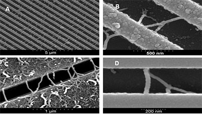
Figure 1. SEM images of: A) trench patterned Si, with stamped 0.1% catalyst solution. MWNTs grown under CVD conditions: 800°C; 0.5 slm of Ar; 0.05 slm C2H2 for 60 minutes. Resulting in ~ 0.6 interconnects per µm of trench length with 18% branch structures and B – D) selection SEM images of straight and branch structure interconnects grown under various CVD conditions.
The sample was left in the reaction chamber for 120 minutes at 800°C in an argon atmosphere. The trenches in the region measured were 420 nm wide, and a 0.1% catalyst solution was drop cast and dried on the substrate surface prior to the experiment. This resulted in an average interconnect growth density of ~0.6 interconnects per micron of trench length with 18% of the total interconnects being of junction structures.
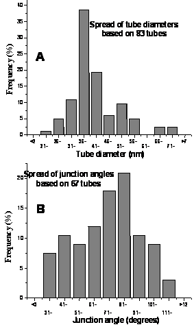
Figure 2. Statistical frequency of A) MWNT diameter (including gold coating (10 nm) to prevent charging effects during SEM) and B) junction angle, taken for a variety interconnects over all tested growth conditions.
Branch Structure Multi Wall Nanotubes
The majority of the branch structure MWNTs grown are Y-junctions though structures with multiple junctions and branches have been recorded (Fig. 1C & D). Through a systematic study of the contributing conditions the optimum conditions used thus far achieved a maximum interconnect density of 1.6 interconnects per micron of trench length with 38% of these appearing to be junction structure MWNTs. These results were achieved with a flow rate of 0.05 slm mixed with argon flowing at 0.5 slm at 700°C for 107 minutes. Of the 199 interconnects measured over a total combined trench length 125.4 µm of which 76 were seen to be branch structures. Though higher proportions of junction structure MWNTs (up to 92%) the number of total interconnects per µm tends to be much lower (0.42 interconnects per µm), so the conditions cited give the highest density of junction structure MWNTs (0.6 junction structures per µm).
A correlation of all data collected (Fig. 2) shows that over all conditions the average tube diameter as measured in the high resolution SEM is 30 – 45 nm. However when one accounts for the gold layer sputtered on to counteract charging effects during electron microscopy the average diameter is reduced to be between 20 – 35 nm. The overall trend for junction structure angles is not as sharp but shows that the majority are between 60 – 90°, which correlates well with what is reported elsewhere(11,20,21).
Reaction Temperature and Trench Width
A more rigorous analysis of the results of the systematic study showed that conditions such as reaction temperature and trench width had a significant effect on the resultant MWNT growth (Fig. 3). It was found that there is an optimum trench width at around 300 nm (Fig. 3A) which gives a maximum for interconnect density per µm of trench length. However it was noted that trench width did not appear to have any noticeable effect on the proportion of junction structure MWNTs.
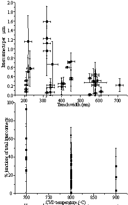
Figure 3. Statistical plots over all conditions of A) interconnects per unit micron length of trench with respect to trench with and B) proportion of total interconnects that are junction structures with respect to CVD operation temperature.
Temperature was found to be one of the conditions with most effect on resultant growth density. It was found that both the number of interconnects per µm and the proportion of junction structures increased with decreasing temperature over the range measured (Fig. 3B).The latter relationship is important as it points the way to a possible mechanism for the formation of the junction structures; the probability of having defects in carbon nanotubes increases with decreasing temperature, giving rise to the possibility that these defects are the seed sites for junction formation.
Raman Spectroscopy
A Raman spectroscopy study was carried out on the samples after CVD which showed that samples containing high proportions of junction structure MWNTs displayed a significantly larger D-band than samples containing a lower proportion of junction structures (Fig. 4). This again suggests that junction structure MWNTs tend to occur when there is a high degree of defects present in the tubes.
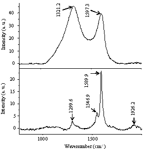
Figure 4. Raman spectra of samples after CVD treatment of areas with A) high proportion of junction structures and B) higher overall MWNT tube growth but lower proportion of junction structures.
Chemical Vapour Deposition
Samples were prepared by CVD on plain Si/SiO2 substrates in order to attain higher densities of MWNTs. These tubes were removed from the surface by sonication in isopropyl alcohol and the suspension examined by TEM (Fig 5). Several examples of junction structures were found displaying similar dimensions and junction angles to those measured during the SEM study.
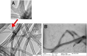
Figure 5. Examples of Junction structure MWNTs under A) TEM and B) STEM
Further TEM investigation (Fig. 6) revealed that the tubes grown under our CVD conditions appear to carry an amount of the catalyst at or near the tip of the tube as they grow out from the original seed particle (Fig. 5A-C). It was also noted that in several cases when kink defects occurred near the end of the tube that some of the catalyst metal appears to be caught at this point (Fig. 5D), this fits well with the observation that the proportion of junction structure MWNTs increases with decreasing temperature to suggest that these kink defect are possible junction seed sites.
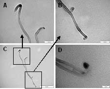
Figure 6. (A – C) TEM images showing two overlying MWNTs, both with two closed ends and possible metal catalyst particles at each end suggesting bottom up tube growth. (D) TEM image of a kink defect in a MWNT containing metal catalyst.
Conclusions
In conclusion we report a method of growing ordered arrays of interconnect type MWNTs with the ability to fine tune the proportion of junction structures through control of initial conditions such as trench width and reaction temperature.
Acknowledgements
This work was supported by the EU Specific Targeted Research Project DESYGN-IT (No NMP4-CT-2004-505626) and with financial support of Intel Ireland, Enterprise Ireland and the HEA.
|
|
1. M. R. Falvo, G. J. Clary, R. M. Taylor, V. Chi, F. P. Brooks Jr, S. Washburn, and R. Superfine, Nature 389, 582 (1997).
2. V. A. N. S. A. Chesnokov, A. G. Rinzler, R. E. Smalley, J. E. Fischer,, Phys. Rev. Lett. 82, 343 (1999).
3. J. W. G. Wildoer, L. C. Venema, A. G. Rinzler, R. E. Smalley, and C. Dekker, Nature 391, 59 (1998).Hench L.L. and Wilson J., “Introduction”, Am Introduction to Bioceramics, Hench L.L. and Wilson J. Eds, World Scientific, Singapore, pp. 1-24, 1993.
4. M. J. Biercuk, M. C. Llaguno, M. Radosavljevic, J. K. Hyun, and A. T. Johnson, App. Phys. Lett. 80, 2767 (2002).
5. L. Huang, W. S. J, and S. P. O’Brien, Nano Lett. 3, 299 (2003).
6. N. Franklin and H. J. Dai, Adv. Mat. 12, 890 (2000).
7. S. Huang, L. Dai, and A. Mau, Physica B, 336 (2002).
8. S.-H. Tsai, C.-T. Shiu, S.-H. Lai, and H.-C. Shih, Carbon 40, 1597 (2002).
9. D. Liu, J. Chen, W. Deng, H. Zhou, and Y. Kuang, Mat. Lett. 58, 2764 (2004).
10. P.-X. Hou, S. Bai, C. Liu, and H.-M. Cheng, Carbon 41, 2477 (2003).
11. B. Gan, J. Ahn, Q. Zhang, Rusli, S. F. Yoon, J. Yu, Q.-F. Huang, K. Chew, V. A. Ligatchev, X.-B. Zhang, and W.-Z. Li, Chem. Phys. Lett. 333 23 (2001).
12. J. Li, C. Papadopoulos, and J. Xu, Nature 402, 253 (1999).
13. G. S. Duesberg, A. R. Graham, F. Kreupl, M. Liebau, R. Seidel, E. Unger, and W. Hoenlein, Diam. Relat. Mater. 13, 354 (2004).
14. A. P. Graham, G. S. Duesberg, R. Seidel, M. Liebau, E. Unger, F. Kreupl, and W. Honlein, Diam. Relat. Mater. 13, 1296 (2004).
15. R. Seidel, A. P. Graham, E. Unger, G. S. Duesberg, M. Liebau, W. Steinhoegl, F. Kreupl, and W. Hoenlein, Nano Lett. 4, 831 (2004).
16. A. N. Andriotis, M. Menon, D. Srivastava, and L. Chernozatonskii, Phys. Rev. B 65, 165416 (2002).
17. D. Zhou and S. Seraphin, Chem. Phys. Lett. 238, 286 (1995).
18. S. Tsai, C. Shiu, W. Jong, and H. Shih, Carbon 38, 1899 (2000).
19. E. Lahiff, C. Y. Ryu, S. Curran, A. I. Minett, W. J. Blau, and P. M. Ajayan, Nano Lett. 3, 1333 (2003).
20. J.-M. Ting, T.-P. Li, and C.-C. Chang, Carbon 42, 2997 (2004).
21. L. P. Biro, Z. E. Horvath, G. I. Mark, Z. Osvath, A. A. Koos, A. M. Benito, W. Maser, and P. Lambin, Diam. Relat. Mater. 13, 241 (2004).
|