Nov 6 2013
A new international research collaboration will deliver highly accurate measurements of strain in materials at the nanoscale to drive innovation in next generation electronic devices. The European Metrology Research Programme's Nanostrain project, led by the National Physical Laboratory (NPL), brings together public institutions from across Europe supported by global industry leaders including IBM.
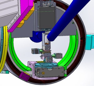 Interferometer and sample holder fitted on a Huber diffractometer (image courtesy of NPL and Huber Diffraktionstechnik GmbH)
A particular focus for the consortium is a class of materials (piezoelectrics) that change their shape in response to electric voltages. The project aims to advance commercial opportunities arising from controlled strain in nanoscale piezoelectrics including the development of the first Piezoelectric-Effect-Transistor (PET), a new digital switch with the potential to offer increased speed, reduced microchip size and lower power consumption.
Advances here would overcome a decade of stagnation in semiconductor transistor performance which has seen computational processing power fail to increase by more than a few percent since 2003. However, progress is dependent on the development of new and more accurate measurements and best practice to better understand strain at the nanoscale and how it can be exploited.
To address this 'final piece of the jigsaw' the European Metrology Research Programme's three year Nanostrain project brings together several European national laboratories along with a consortium of collaborators including world-class research instrument facilities at the European Synchrotron Radiation Facility (ESRF) and nine commercial companies spanning a wide range of applications.
The project will develop new tools for the characterisation of nano-strain under industrially relevant conditions of high stress and electric fields. The results will then be openly available to manufacturers and designers to encourage innovation across a wide range of industries.
Professor Markys Cain, Nanostrain project lead at NPL, said:
"This is a completely unique collaboration, unparalleled in terms of its collective expertise in the areas of material science, metrology and the properties and performance of piezoelectric systems. It's an exciting project to be involved in as it won't be simply going over old ground or providing a minor improvement on what already exists. Currently there is no metrological framework or facilities for traceable measurement in this area. This is high risk, challenging work that will underpin a major step change in the performance of devices we use every day and bring highly influential new technologies to market in diverse sectors such as microelectronics, ICT, 3D printing and sensors industries."
This work is funded through EURAMET's European Metrology Research Programme (EMRP) Project IND54 Nanostrain. The EMRP is jointly funded by the EMRP participating countries within EURAMET and the European Union.