|
It is well documented that carbon nanotubes have a huge variety of potential applications. This is due to their high electrical and thermal conductivities, exceptional strength, stiffness and ability to regain their original shape after compression [2-5]. Carbon nanotubes can be grown by different processes which include; arc discharge, laser ablation and chemical vapour deposition. The most promising of these techniques is CVD which allows CNTs to be grown in situ on pre-patterned substrates [6]. While patterning is conventionally done by photolithography, recently a new method called soft lithography patterning has been demonstrated to be more efficient, economical and versatile [7-10]. Nanotubes are of tremendous interest both in their original form, and also as part of a composite material. Embedded nanotubes in polymer matrices enhance the material properties by increasing mechanical strength and conductivity [11-13]. However, when composite formation is carried out in solution, CNTs usually form aggregates which have reduced properties in comparison with individual tubes. Also, for optimal load transfer from the polymer to the embedded CNTs, there must be a strong interface between the tubes and the matrix. These are but two of the problems associated with CNT-polymer composite production and they have been addressed by many research groups. Possible solutions include plasma treatment leading to enhanced dispersion [14] and functionalisation of the CNTs [15]. Successful incorporation of CNTs in polymer matrices could lead to applications including; flat panel displays, sensors, flexible electronic devices, and actuators [16-18]. Before realizing their full potential, the issues of controllable and economic production of nanotubes and their subsequent composites, must be overcome.
We have previously reported an efficient and cost effective method of incorporating carbon nanotubes into a poly(dimethylsiloxane), PDMS, polymer matrix [1] . Using this technique we were able to incorporate as-grown CNT arrays into a composite. This eliminates the need to disperse the CNTs prior to composite formation. It also allows control over the position and density of the embedded nanotubes. The morphology of the embedded nanotubes can be controlled by altering the CVD conditions used to grow the CNTs [19].
Here we describe the subsequent direction of our research which is to vary the volume fraction of CNTs in a reinforced polymer. This is done by growing CNT arrays in grid patterns. Previously we reported using parallel lines of CNT arrays which strengthen only in the direction parallel to the lines. Grid patterns however allow for mechanical reinforcement in both the x- and the y-plane of a thin film composite. In general the grid lines are 5μm wide and the separation between lines is increased to vary the volume fraction of CNTs grown on the substrate surface. We will then use these as-grown CNTs to reinforce polymer thin films by spin coating a curable polymer onto the nanotube grids.
Experimental
Carbon nanotubes were grown by CVD using acetylene, C2H2, as the carbon source. Substrates used for nanotube growth were prepared by soft lithography patterning as described elsewhere [20-22]. This technique employs the use of an elastomer stamp, to pattern a catalyst solution onto a silicon oxide substrate. The stamp is cast from a silicon master patterned by conventional photolithography techniques (Figure 1A).
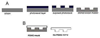
Figure 1. (a): Schematic of patterning a silicon master using traditional photolithography. (b): Schematic of casting an elastomer stamp from a silicon master. The stamp can then be used for soft lithography patterning. Many stamps can be cast from the same master.
Photolithography Patterning
The first step in photolithography patterning of the master was to design a positive chrome on high grade quartz, 4inch x 4inch x 0.06inch photomask. The mask was designed using Kic 2.4 software [23] and then manufactured by Photronics (Wales) Ltd. The design we chose was grid patterns with incremental spacing between grid lines. The position of grid lines corresponds to the eventual location of CNT arrays. Hence, we systematically decrease the volume fraction of CNTs grown on the substrate surface by increasing the inter-grid spacing. It is intended that these CNT grid patterns be incorporated into thin film composites. We will therefore have a method of controlling the volume fraction of nanotubes embedded within a polymer matrix. It is the location and density of embedded nanotube networks that determine the mechanical, electrical and thermal properties of the composite material. Gridlines were designed to be 5ƒÊm wide with separations from 5μm to 75μm.
Photomask
This photomask was then used to transfer the grid pattern onto a silicon master. A silicon wafer was first cleaned using a peroxide/sulphuric acid solution (H2SO4:H2O2 in the ratio of 3:1) and pre-baked to remove any residual water. Next a layer of HMDS (hexamethyldisilazane), adhesion promoter was spin cast onto the silicon followed by Shipley 1813 positive photoresist. The photomask was placed over the photoresist and unmasked areas were depolymerised by exposure to UV. After UV exposure, Shipley MF 319 developer was used to remove areas of photoresist which had degraded. The pattern was transferred by reactive ion etching, RIE, of the exposed silicon. RIE involved the use of CF4 gas at a flow rate of 50 standard cubic centimeters per minute (sccm), rf power at 100W and a pressure of 1 Torr. The etch time was 15min. The etched master was imaged by Field Emission Scanning Electron Microscopy (FESEM) and a height profile was obtained by interferometry.
Elastomer Stamps
The next step was to cast elastomer stamps from this silicon master. The elastomer used is poly(dimethylsiloxane), PDMS, (Dow Corning). This is a hydrophobic polymer and will adhere strongly to the silicon master. The reason for this irreversible sealing is the formation of covalent -O-Si-O- bonds by a condensation reaction of the silanol groups on the PDMS and the -OH-containing functional groups on the silicon. Hence we must make the master hydrophobic before casting the stamps. This is done using fluorosilane as a release promoter. First the silicon master is cleaned and activated by UV/ozone for 30mins. Immediately after activation, the substrate is placed in a dessicator together with about 0.3-0.5 ml (heptadecafluoro-1,1,2,2-tetrahydrodecyl)-trichlorosilane, (Oakwood Products Inc.). The dessicator is pumped down to a pressure of 2.0 mbar. After 60 minutes the dessicator is vented with air. The substrate is then inserted into a preheated oven at 60ºC for 45min.
PDMS Elastomer Stamps
PDMS elastomer stamps were cast from the hydrophobic silicon master (Figure 1B). A mixture of PDMS base: curing agent, in a 10: 1 ratio, was drop cast onto the master and allowed to cure under atmospheric conditions over a period of 4 days. The cured PDMS stamps then released easily from the master and as expected, the stamps displayed the inverse topology of the masters. This was verified by interferometry. Stamps were in the region of 1cm thick.
Catalyst Patterning
The stamps were then used to pattern an iron containing catalyst for CNT growth. Poly(styrene-vinylferrocene), was anionically synthesized by the authors, and characterized by Nuclear Magnetic Resonance and Gel Permeation Chromatography (not shown) to determine its iron content (2.1%). Thermal Gravimetric Analysis showed that between 350ºC and 450ºC, 93% of the polymer decomposed. It also confirmed that 4% of the catalyst particles (presumably iron or iron oxide) remained at 800º‹C. Hence, this catalyst was suitable for use in CVD CNT growth, which was determined previously to be optimal at 700ºC [19].
The PS-PVF catalyst was patterned onto 100nm SiO2, which is sufficiently above the critical thickness of 50nm where NT growth velocity saturates [24]. CVD was performed under argon at atmospheric pressure. The argon carrier gas flow rate was 200sccm. The active gas used was acetylene. The flow rate for acetylene was 200sccm. CNTs were grown at 700ºC (at 800ºC carbon fibers with diameters greater then 100nm form) and deposition time can be varied from 10min to 1hr depending on the length of CNTs required.
Results and Discussion
Grid patterns were etched into a silicon master (Figure 2). The 4inch x 4inch master was separated into 15 sections. Each section contained 5μm grid patterns with spacings ranging from 5-75μm. This corresponded to volume fractions from 12-92%.
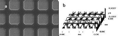
Figure 2. FESEM (a) shows a silicon master displaying grid patterns. Interferometry (b) shows the height profile of the master.
The master was then treated with fluorosilane to form a surface with low interfacial free energy. The contact angle was measured to change from an average of 16º ± 2º to an average value of 114º ± 6º, which was stable for more than 45 days. Elastomer stamps were then cast from the master and released easily. Interferometry showed that the depth of the features on the stamps was 492nm (Figure 3). These stamps were used as produced and no further treatment was necessary. Previous methods [7,8,10] have described the hydrophilization of PDMS stamps to make them compatible with catalyst solutions to be patterned. This step is unnecessary with our catalyst material.
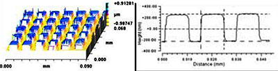
Figure 3. An interferometry scan shows the surface topology of the stamp and gives a height profile of 492nm.
The stamps were used to pattern a catalyst solution onto SiO2 substrates. The catalyst used was poly(styrene-vinylferrocene), PS-PVF. The vinylferrocene part of this polymer contains an iron core which is active as a catalyst for CNT growth at the temperatures used in these experiments. The PS-PVF polymer powder was dissolved in toluene. Initially tetrahydrofuran was used as the solvent but, we obtained enhanced pattern quality by using toluene. Toluene reportedly swells PDMS [22] but for our 5μm feature sizes we found no adverse effects on the pattern quality. We were also able to re-use the PDMS stamps a number of times before pattern quality began to degrade. We used a 4wt% solution (varying the concentration of the solution can be used as a method to control the density of nanotube growth [19]). A drop of PS-PVF solution was placed on the SiO2 substrates. The elastomer stamp was then brought into contact with the substrate. The catalyst solution migrates into the grooves on the stamp, it was left overnight for the toluene to evaporate and when the stamp was removed it revealed a patterned substrate as shown in Figure 4.
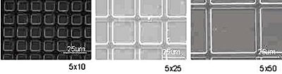
Figure 4. Catalyst micro-patterns generated by soft lithography patterning. The spacing between gridlines is 10, 25 and 50μm (left to right). The width of the gridlines is constant at 5μm.
Soft lithography patterning allows us to confine the catalyst particles to within the dimensions of our patterns. Therefore during CVD we would expect that the CNTs grow only within the dimensions of the grids which was observed in Figure 5.
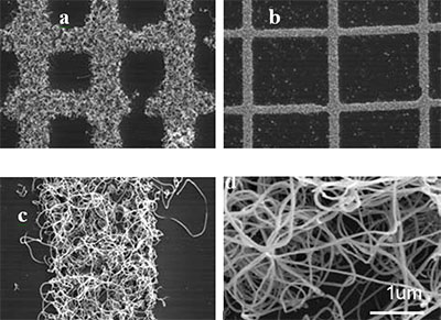
Figure 5. After CVD, carbon nanotube growth occurred only on the micro-patterned areas of the substrate. CNTs were grown on grids with 10μm (a) spacing and 50μm spacing (b). (c) and (d) show a higher magnification of the nanotubes grown within the dimensions of the grids.
Conclusions
In conclusion, we report a scalable inexpensive technique to grow grid patterns of nanotube arrays. The inter-grid spacing can be tailored as required giving a simple method of controlling the volume fraction of nanotubes grown on our substrates. It is our intention to incorporate these CNT arrays into a flexible free-standing thin film composite. To do this we will employ a novel method of composite production previously described and demonstrated by the authors.
Using soft lithography patterning we can selectively position the CNT conduction channels and control their volume fraction within the composite. The composite can then be used for applications which require conductive channels within a bendable matrix. These applications include flexible electronics, electromagnetic shields and sensors.
Acknowledgments
The authors acknowledge the Irish Higher Education Authority (HEA), Enterprise Ireland and the EU Specific Targeted Research Project DESYGN-IT (No NMP4-CT-2004-505626) for financial support.
The authors are also grateful to Prof. P.M. Ajayan and Prof. C.Y. Ryu, of Rensellaer Polytechnic Institute, New York, and also, Prof. S. Curran of New Mexico State University, for their initial input into this project.
|
|
1. E. Lahiff, C.Y. Ryu, S. Curran, A.I. Minett, W.J. Blau, P.M. Ajayan, Nano Lett. (Communication), 3(10), 1333-1337, 2003.
2. M. R. Falvo, G. J. Clary, R. M. Taylor, V. Chi, F. P. Brooks Jr, S. Washburn, R. Superfine, Nature, 389, 582, 1997.
3. J.W.G. Wildoer, L.C. Venema, A.G. Rinzler, R.E. Smalley, C. Dekker, Nature, 1998, 391, 59.
4. M.J. Biercuk, M.C. Llaguno, M. Radosavljevic, J.K. Hyun, A.T. Johnson, Appl. Phys. Lett., 2002, 80, 2767.
5. S. A. Chesnokov, V. A. Nalimova, A. G. Rinzler, R. E. Smalley, J. E. Fischer, Phys. Rev. Lett., 82 (2), 343, 1999.
6. B. Q. Wei, R. Vajtai, Y. Jung, J. Ward, R. Zhang, G. Ramanath, P. M. Ajayan, Nature, 416, 495, 2002.
7. H. Kind, J.M. Bonard, C. Emmenegger, L.O. Nilsson, K. Hernadi, E. Maillard-Schaller, L. Schlapbach, L. Forro, K. Kern, Adv. Mater., 11 (15), 1285, 1999
8. J.M. Bonard, P. Chauvin, C. Klinke, Nano Lett., 2 (6), 665-667, 2002
9. S. Huang, L. Dai, A. Mau, Physica B, 323, 333-335, 2002.
10. H. Kind, J.M. Bonard, L. Forro, K. Kern, K. Hernadi, L.O. Nilsson, L. Schlapbach, Langmuir, 16, 6877-6883, 2000.
11. M. Cadek, J. N. Coleman, K.P. Ryan, V. Nicolosi, G. Bister, A. Fonseca, J.B. Nagy, K. Szostak, F. Beguin, W.J. Blau, Nano Lett., (Communication), 4(2); 353-356, 2004.
12. J. N. Coleman, M. Cadek, R. Blake, V. Nicolosi, K. P. Ryan, C. Belton, A. Fonseca, J. B. Nagy, Y. K. Gun'ko, W. J. Blau, Adv. Fun. Mater., 14 (8), 791-798, 2004
13. A.B. Dalton, S. Collins, E. Munoz, J.M. Razal, V.H. Ebron, J.P. Ferraris, J.N. Coleman, B.G. Kim, R.H. Baughman, Nature, 2003, 423, 703.
14. D. Shi, J. Lian, P. He, L.M. Wang, F. Xiao, L. Yang, M.J. Schulz, D.B. Mast, Appl. Phys. Lett., 83 (25), 5301, 2003.
15. Velasco-Santos, A.L. Martýnez-Hernandez, F.T. Fisher, R. Ruoff, V.M. Castan, Chem. Mater., 15, 4470-4475, 2003.
16. W.A. de Heer, A. Chatelain, D. Ugarte, Science, 1995, 270, 1179.
17. A. Modi, N. Koratkar, E. Lass, B. Wei, P.M. Ajayan, Nature, 2003, 424, 171.
18. S. Courty, J. Mine, A. R. Tajbakhsh and E. M. Terentjev, Europhys. Lett., 2003, 64 (5), 654–660.
19. E. Lahiff, A.I. Minett, S. Curran, C.Y. Ryu, W.J. Blau, P.M. Ajayan, Mat. Res. Soc. Symp. Proc., Vol. 782, A5.11.1, 2004.
20. Y. Xia, G.M. Whitesides, Angew. Chem. Int. Ed., 37, 550-575, 1998.
21. Y. Xia, J. Tien, D. Qin, G.M. Whitesides, Langmuir, 12, 4033-4038, 1996.
22. A. Kumar, G. M. Whitesides, Appl. Phys. Lett., 63 (14), 2002-2004, 1993.
23. IC Design Software, Whiteley Research Inc., 456 Flora Vista Avenue, Sunnyvale CA 94086.
24. A. Cao, P.M. Ajayan, G. Ramanath, R. Baskaran, K. Turner, Appl. Phys. Lett., 84 (1), 109, 2004
|