Sponsored by HORIBAMay 20 2008
A photovoltaic cell, or solar cell is a semiconductor device consisting of a large-area p-n junction diode that in the presence of sunlight is capable of generating usable electrical energy. This conversion is called the photovoltaic effect. Solar cells have many applications, and are particularly well suited to situations where electrical power from the grid is unavailable, such as in remote area power systems, Earth orbiting satellites, handheld calculators, remote radiotelephones, water pumping applications, etc.
Much of the research is focussed on making solar cells cheaper and more efficient, so that they can more effectively compete with other energy sources. Much of this optimization requires accurate characterization of film thickness and absorption efficiency for the thin films used to manufacture the cells.
Spectroscopic ellipsometry is an optical measurement technique used to determine thin film thickness and optical constants simply and accurately. This article illustrates the ability of the technique to characterize photovoltaic devices. The materials commonly studied include: amorphous silicon, poly silicon, ZnO, ITO, SnO2, TiO2, SiNx, MgO, etc.…
The Photovoltaic Cell – How Does It Work?
The photovoltaic effect starts with the absorption of photons in a semiconductor above its energy band gap, leading to the generation of charge carriers (electrons and holes). These charge carriers are then separated by an internal electric field created either by a p-n or p-i-n junction within the semiconductor, or by a hetero-junction between the semiconductor and another material.
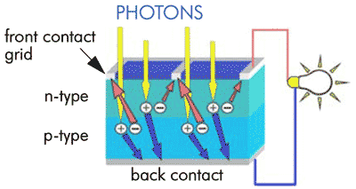
Figure 1. Diagram of a photovoltaic cell.
Finally the charge carriers are collected by electrodes and can be used to generate a current in the outer circuit. The front electrode of the cell should be designed to allow high transmission of photons. This can be accomplished either by a fine grid of metal, or by using a transparent conductive oxide (TCO) such as Indium-Tin-Oxide (ITO), Tin-Oxide (SnO2) or Zinc-Oxide (ZnO). Antireflection coatings, used to increase the amount of light coupled into the solar cell, are typically deposited on the front side of the cell. It is typically applied in a layer several hundred nanometers thick using plasma enhanced chemical vapor deposition (PECVD).
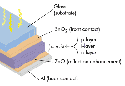
Figure 2. Schematic cross-section of thin film a-Si:H photovoltaic cell.
Materials and Efficiency
Various materials have been investigated for solar cells. Most large-scale commercial solar cell factories manufacture screen printed poly-crystalline silicon solar cells. Single crystalline wafers can be made into excellent high efficiency solar cells, but they are generally considered to be too expensive for large-scale mass production. Amorphous silicon cells have low conversion efficiencies of around 8%. Polymer or organic solar cells are built from ultra thin layers (typically 100 nm) of organic semiconductors. They are potentially cheaper to manufacture than silicon, but efficiencies achieved to date are low and cells are highly sensitive to air and moisture, making commercial applications difficult.
Photovoltaic Device Characterization
Three examples of samples commonly characterized by spectroscopic ellipsometers are presented below. The analysis were performed using a HORIBA UVISEL spectroscopic phase modulated ellipsometer controlled by DeltaPsi2 software. Ellipsometric data were acquired at an angle of incidence of 70°, across the extended spectral range from 0.6 to 6.5 eV (190 – 2100 nm).
Graded Microcrystalline Silicon Layer
The microcrystalline silicon layer is inhomogeneous in depth. The model includes a graded layer (linear function) used to specify one value at the bottom of the layer and another one for the layer top. The optical constants of the microcrystalline silicon were represented using a dispersion formula.
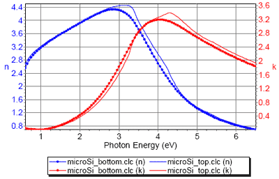
Figure 3. Optical constants of microcrystalline silicon.
The result obtained shows the excellent agreement between the model (line) and the experimental data (dots) on the whole spectral range, with ?2 =0.81 (result quality parameter).
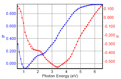
Figure 4. Experimental and generated data.
Inhomogeneous ZnO Layer
The sample consists of a ZnO layer deposited on c-Si. To represent the inhomogeneity in depth of the ZnO layer, a three layer model was used. The sample exhibits a small roughness on top, and the density of the ZnO increases from the c-Si interface (1st layer) to the top (2nd layer). It provides an increase of the refractive index from the 1st to the 2nd layer.
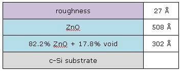
Figure 5. Optical constants of ZnO
Thickness Mapping of SiNx Layer
By using a motorized XY sample stage and a mapping recipe it is simple to automate the analysis at different positions on the sample. Both thicknesses and optical constants were determined at each points. The mapping shows a variation of SiNx thickness between 600 and 750 Å over the surface of the sample.
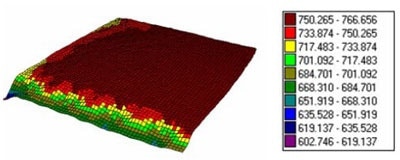
Figure 6. Thickness map of SINx Layer
Conclusion
Spectroscopic ellipsometry is an ideal technique to characterize film thicknesses and optical constants for photovoltaic applications. Spectroscopic ellipsometers are also sensitive to the presence of rough overlayer and graded optical constants. The technique provides the advantage to be fast, simple to operate and non-destructive for the characterization of the samples.

This information has been sourced, reviewed and adapted from materials provided by HORIBA.
For more information on this source, please visit HORIBA