WITec manufactures high-performance instrumentation for scientific and industrial applications focused on novel solutions for optical and scanning probe microscopy. This article describes the analysis of stress fields around a Vickers indent using optical and scanning probe microscopy.
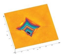
Figure 1. AFM image.
The stress field around a Vickers indent was examined by utilizing the relative shift of the 520/cm Si-Raman line. The Vickers indent was conducted with a force of 50mN, resulting in a pyramidal hole of 2,75ìm diagonal size and 210nm depth, as shown in Figure 1.
Topography Images around Vickers Indent
Figure 2 shows a comparison of the topography (5x5ìm, 5nm vertical scale, left) around the Vickers indent resulting stress image of the same area acquired in Raman imaging mode (10x10ìm scale, right). The AFM image’s area is marked for a clearer comparison.
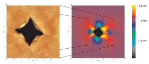
Figure 2. Comparison of the topography (5x5ìm, 5nm vertical scale, left) around the Vickers indent and a subsequent stress image of the same area.
Stress Images around Vickers Indent
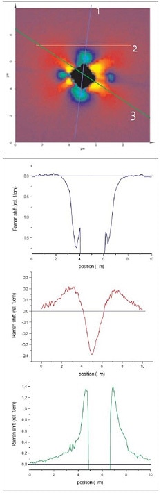
Figure 3. The position of three cross sections (labelled 1-3) on top and displayed on the right (1: top, 3: bottom).
In Figure 3, the location of three cross sections (labelled 1-3) are highlighted in the stress image on top and shown on the right (1: top, 3: bottom). As anticipated, the stress field exhibits the symmetry of the Vickers pyramid. The compressive strain (yellow in the stress image) appears at the flat sides, whilst the tensile strain (blue in the stress image) appears at the borders of the pyramid.
Raman Images
The Raman image is acquired by rotating the turret from the AFM objective to a normal optical microscope objective (Nikon, 100x, NA=0.9 NCG) without shifting the sample. As can be seen, the stress field extension can be easily identified more than 5ìm from the middle of the indent. The stress image (100x100=10.000 spectra) was acquired with 10mW excitation power (532nm) and merely 70ms integration time per spectrum.
Accuracy of Stress Measurements
The extreme precision of the stress measurement are shown in the cross sections with a standard deviation of just 0,021/cm. This precision was achieved by ascertaining the peak position of a parabolic fit to the Si-Raman line of each measured spectrum and with an integration time of just 70ms per spectrum.
An even higher degree of precision can be obtained with longer integration times. Since the relation between peak shift and stress for silicon is (MPa) = -435 (1/cm), a 0.02/cm accuracy corresponds to a stress sensitivity of only 9MPa.
Conclusion
WITec’s optical and scanning probe microscopy Instruments can be effectively used for identifying the stress Images around a Vickers indent.

This information has been sourced, reviewed and adapted from materials provided by WITec GmbH.
For more information on this source, please visit WITec GmbH.