Using photovoltaic devices to generate energy is considered an essential component to overcome future energy shortages. This is reflected in a drastic increase in photovoltaic production and demand. While conducting research and development of PV devices, the key goals are to increase the conversion efficiency of the solar cells or to enhance the production process. Confocal Raman imaging is an important tool for these studies as it does not just reveal optical information but also data with regards to the 3D distribution of the chemical compounds, material stress, and crystallinity.
In a joint research project, the ISE (Durability Analysis and Environmental Engineering Group) studied a number of solar cell samples relevant to the solar cell industry using Confocal Raman Microscopy. This article enumerates the application of confocal Raman imaging for analyzing stress fields around laser-drilled holes on a Si solar cell as well as the examination of concentration-dependent properties of a dye solar cell.
Stress Fields surrounding Laser-drilled Hole on Si Solar Cell Device
Typical Si-based solar cells are mainly built as shown in Figure. 1.
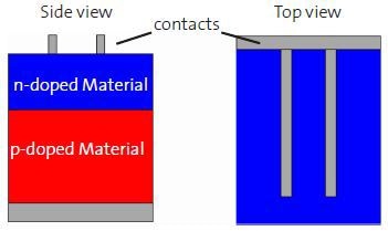
Figure 1. Typical set-up of a solar cell.
Positioning of the discharging contacts is done on the p and n doped material. Contacts are normally not placed on the upper surface as they tend to block some of the sunlight and hence lower the efficiency. It is hence important to drill holes through the solar cells to permit the contacts to be located on the bottom of the solar cells. These holes are drilled with lasers.
Two ways of minimizing stress are investigated in this study:
- Minimizing the laser power for drilling using 100% drilling power with 9 repetitions or 20% drilling power with 20 repetitions
- Etching the wafer follwing the drilling process with the options of no etching, 1 Minute etching with KOH, 2 Minutes etching with KOH, 4 Minutes etching with KOH and, 6 Minutes etching with KOH.
Confocal Raman imaging was used to evaluate the strain induced by the drilling on the Si around the holes. These measurements were performed with a WITec alpha700 system using a 532nm excitation laser, a 100x air objective (NA 0.9).
A 50µm core diameter multi-mode fiber was used to direct the scattered light to the spectrometer, which also serves as the pinhole for confocal detection. The spectrometer was a WITec UHTS 300 fitted with an 1800 grooves/mm grating and a back-illuminated CCD camera. For each spectrum, the integration time was 23ms and 150x150 pixels (22500 spectra) over an area of 35x35pm. The total acquisition time per image was below 10 minutes.
Certain holes showed Si splashes on the wafer surface which resulted in a higher 1st order Si peak on these structures as illustrated in Figure 2, where the integrated intensity of the Si peak is assessed at each pixel and displayed as an image.
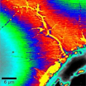
Figure 2. Splash of Si onto the surface out of the hole (bottom right). Plotted is the integrated intensity of the 1st order Si peak.
Figure 3 shows holes with relatively smooth surroundings.
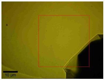
Figure 3. Video Image of a typical scan area (red box) on the SI. The hole is visible on the bottom right corner.
For each image, the 1st order Si peak was fitted utilizing a Lorentzian curve and the actual peak position was then assessed. This could also be shown as an image and an example is shown in figure 4. From these images, cross-sections as shown in Figure 4 were extracted and plotted as relative peak positions (in rel.1/cm) vs. distance. Figures 5 and 6 display the results of these evaluations. Figure 5 depicts the results for the samples with full drilling power and the different etching processes applied to the samples are indicated by the colors [no etching (red), 1 min etching (blue), 2 min etching (green), 4 min etching (black), 6 min etching (magenta)]. Figure 6 employs the same color coding, but shows the results for the cases drilled with just 20% power.
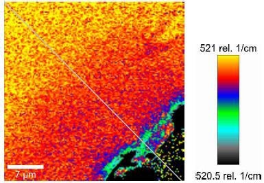
Figure 4. A typical stress map of the Si (Position ofthe ist order Si line) from the outside to the hole (bottom right) Along the indicated cross section (gray line), the radial change ofthe stress field was evaluated.
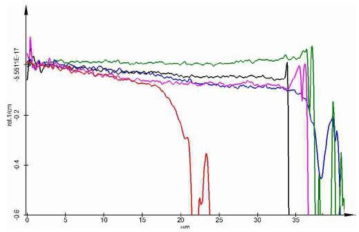
Figure 5. The cross sections of the various samples drilled with 100% laser power: no etching (red), 1 min etching (blue), 2 min etching (green), 4 min etching (black), 6 min etching (magenta).
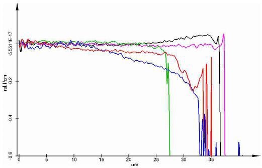
Figure 6. The cross sections ofthe various samples drilled with 20% laser power: no etching (red), 1 min etching (blue), 2 min etching (green), 4 min etching (black), 6 min etching (magenta).
Dye Solar Cells
A test array for observing dye distribution attached to the TiO2 and the evaluation of the iodide in dye base solar cells was prepared (sample courtesy of FraunhoferInstitute for Solar Energy Systems ISE). The concentration of iodide varied in the samples from 0% to 600% of the concentration typically utilized in dye bases solar cells.
The following structure was seen in the investigated cells:
- Glass with Transparent Conductive Oxide, 3mm total thickness
- Inner area (total thickness ca 30-35pm):
- TiO2 nano-porous area (ca. 10pm)
- Ionic liquid (contains single iodide ions)
- Monolayer dye Electrolyte consisting of: *ACN (acetonitril)
- Iodide (varying in concentration and forming tri-iodide-ions).
Conclusion
Confocal Raman imaging can be effectively used to analyze the properties of solar cell materials. This technique reveals optical information as well as information related to the 3D distribution of chemical compounds.

This information has been sourced, reviewed and adapted from materials provided by WITec GmbH.
For more information on this source, please visit WITec GmbH.