Before the production of Scanning Capacitance Microscopy (SCM), semiconductor chip manufacturers, failure analysis engineers, and researchers could not capture the slight errors and variations in mask and implant alignment, doping levels, and device failures as a result of these errors.
The development of SCM enabled engineers to analyze the devices at the sub-micron scale and discern errors both for failure analysis and during device fabrication. The updated SCM design from Oxford Instruments provides these same insights, but with major benefits not included in prior generation designs.
These distinct features provide greater resolution, higher sensitivity, faster imaging, and the direct quantification of capacitance rather than only differential capacitance (dC/dV).
The sensitivity of the circuit additionally enables insulators and metals to be probed, as well as non-linear materials beyond the class of conventional semiconductor devices, such as those that do not form a native oxide.
SCM is a nano electrical AFM imaging method at its essence. It utilizes a microwave radio frequency (RF) signal to analyze the local electrical characteristics of a sample, quantifying free carrier concentrations and types. Variations in capacitance down to 1 aF resolution1 can be identified using SCM.
RF detection has been deployed on scanning probe microscopy systems in a variety of ways. Here, a rather basic but highly sensitive technique to measure the reflected RF signal is outlined.
As outlined in Figure 1, a directional coupler is used to route a microwave signal produced by an RF source to the AFM probe. An RF peak detector measures the reflected microwave signal from the probe-sample junction which is amplified by a two-stage high-gain amplifier.
The measured value (RF Reflection) corresponds to the capacitance of the sample and is displayed as the capacitance data channel. The reflected signal misses the second time attenuation widespread in the majority of current SCM sensor modules by utilizing a directional coupler.
In the outdated SCM circuits, a second time coupling arises between the transmission lines throughout the signal return. This effect is eliminated through the updated circuit design which offers a much greater sensitivity.
The electric charge carriers residing under the surface of the sample are modulated through a reference signal (sample bias) which is applied to the sample. This will normally be p-type or n-type dopant implants, but additional non-linear materials will also react to this modulation.
The capacitance of the sample is altered by this voltage modulation, and the difference in capacitance in relation to voltage is quantified, for example, the differential capacitance dC/dV signal.
The dC/dV lock-in output’s amplitude can be utilized to predict doping density. The phase of the dC/dV output is employed to distinguish the carrier polarity, determining the dopant type as either hole (p) or electrons (n).
The imaginary and real channels of the dC/dV signal can be outputted by determining the lock-in amplifier output -Cap×cos(Θ) and Cap×sin(Θ).
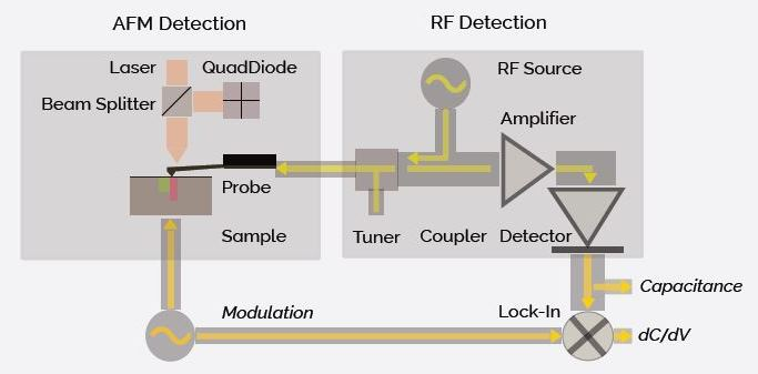
Figure 1. Block diagram of the SCM/AFM design (see the text for details).
It should also be noted that the tip is connected to the ground and the modulation bias is applied to the rear of the sample. This procedure reduces RF circuit interference. In textbooks for semiconductor theory, the bias is normally demonstrated to be applied to the oxide side.
Figure 2 shows the relationship between capacitance and its derivative (dC/dV) while the sample bias undergoes changes.
The positive voltage close to the surface oxide side repels the positive carriers in the p-doped region, which increases the conductance of the semiconductor, and the sample capacitance increases to be close to the oxide capacitance.
An increase in negative voltage in the n-doped regions will move the negative carriers close to the oxide layer, meaning the capacitance increases with negative voltage.
On the dC/dV curves, the n-doped regions of the sample have a negative slope and the p-doped regions have a positive slope. The change in capacitance is less prominent in higher-level doped samples in contrast to lower-level doped samples.
When the sample behaves like a metal and becomes highly conductive, the capacitance goes down to zero.
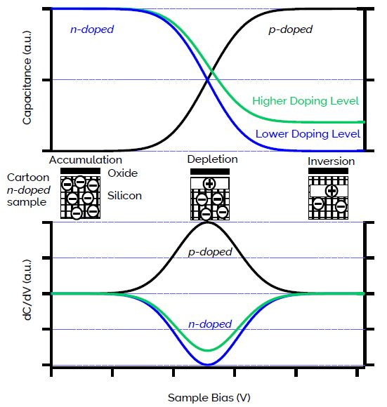
Figure 2. Typical Capacitance C-V and dC/dV spectra on the semiconductor material. In the n-doped sample, the capacitance decreases with increasing sample bias, while it increases in the p-doped sample. At a higher doping level, the capacitance changes slower (top graph). These bias dependent changes are also visible in the dC/dV spectra (bottom graph).
Impedance matching between the RF circuit and the cantilever type is also crucial to this new SCM circuit’s sensitivity. The cantilever impedance is unknown although the RF detection system has a nominal impedance of 50 Ω which means a mechanism for impedance matching must be used.
Here, a single stub matching technique is employed, where two different single stubs are tuned to produce matched circuits with two chosen types of probe.2 Increased sensitivity is achieved through a good impedance match at the operating frequency which reduces the reflected signal and enables increased power to reach the sample.
As demonstrated in Figure 3, a resonance dip in the reflected RF signal can be identified by sweeping the RF source while the detector output is recorded. The detector output value is normally close to zero volts at the minimum reflection.
For the majority of SCM measurements on standard non-linear materials, two separate probe classes are utilized which must be matched individually for sensitivity optimization. The first is silicon probes with a conductive tip-side coating (such as doped/coated diamond probes) and the second is solid platinum probes.3
The resonance frequency shifts lower in relation to the solid platinum probes as the total impedance of coated silicon probes is higher, as displayed in Figure 3.
The signal is enhanced without disturbing the impedance matching when thicker conductive coatings are used. This means that a greater range of probes is available to choose from, unlike existing scanning microwave methods that utilize expensive specialized probes.
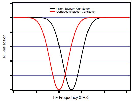
Figure 3. RF tunes for two different types of cantilevers. The frequency shift is caused by the impedance difference of silicon lever vs. platinum lever.
To enhance the detection of dC/dV, the RF operating frequency at which the reflected RF signal has the highest slope is selected for optimal sensitivity.
As demonstrated in Figure 4, the reflected RF signal’s derivative is determined and the minimum or maximum position on the derivative curve is selected as the operating RF frequency, as detailed by the vertical dashed line.
The best RF operating frequency is automatically selected by the SCM software after each cantilever RF tune. This can be further demonstrated by performing an on-surface RF sweep while the dC/dV channel is observed, showing that the operating frequency provides the optimal dC/dV signal.
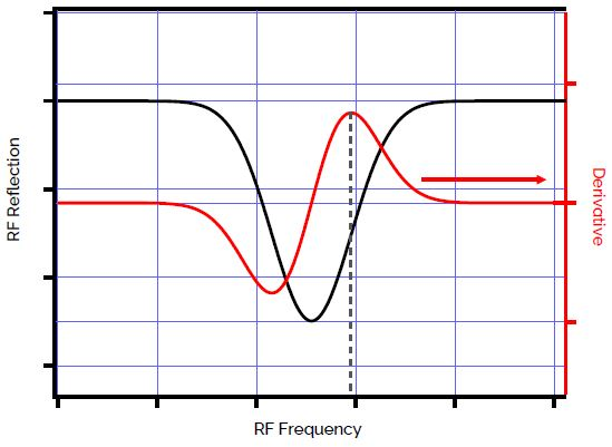
Figure 4. RF tune of the SCM system. The operating RF frequency is automatically chosen by software after the tune.
Examples on Semiconductor Materials
This section presents data acquired from a range of samples utilizing the Asylum Research SCM module. The data demonstrated was taken on both the Cypher AFM and the Jupiter XR large-sample AFM. The initial sample is the static random-access memory (SRAM) sample from Sandia National Laboratories. It is likely to have been imaged using microwave-based imaging methods more than any other sample type.
Figure 5 outlines the four main SCM image channels for the SRAM sample across a 30 μm region. The metal layering has been removed in addition to other features until only the silicon is exposed, and as seen from the top down, the visible structures are transistor devices.
The native oxide is relied upon to enable the sample to behave as a metal-oxide-semiconductor (MOS) capacitor, with the ‘native’ oxide as the oxide, the devices to be the semiconductor material, and the AFM tip as the metal.
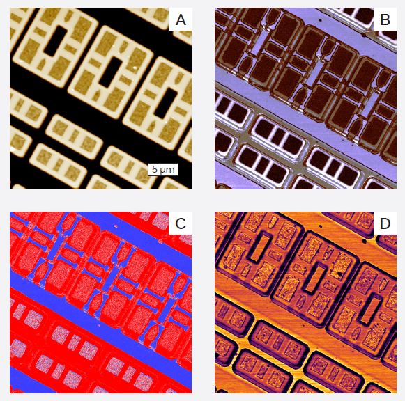
Figure 5. SRAM sample with top-down access to the source, drain, and gates. All of the channels shown were acquired simultaneously and include a) Topography, b) dC/dV Amplitude where brighter areas indicate lower doping and darker indicate higher doping, c) dC/dV Phase where blue indicates p-type doping and red indicates n-type doping, and d) Capacitance, which has a linear correlation with dopant levels.
In Figure 6, which shows a closer analysis of the dC/dV amplitude image, two bright features can be observed which are the channel region underneath the gates. To the lower left and upper right, the darker areas are the sources and the middle area is the drain for each of the devices.
The gates are theoretically 250 nm devices, but errors in the process, surface states, and sample history can alter the stated width of the gate utilizing the SCM method. The width of the gates in this example is measured to be 240 nm.
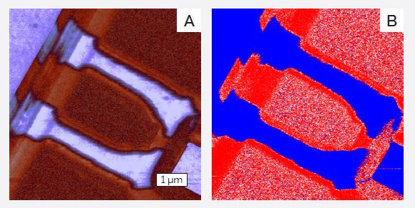
Figure 6. Zoom into the gate feature of the SRAM sample. a) dC/dV Amplitude image showing dopant level and b) dC/dV phase image showing dopant type.
As demonstrated in Figure 7, the design of the new Asylum Research SCM module provides a high bandwidth which allows for the acquisition of high-quality data and at scan rates as fast as 26 Hz.
In contrast, the majority of SCM modules available on the market frequently need scan rates of less than 1 Hz. The high scan rates enable high quality, quick survey scans that can be employed to efficiently determine particular regions of interest (ROI).
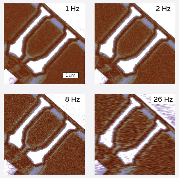
Figure 7. dC/dV Amplitude images acquired on the SRAM sample at increasing scan rates.
Another method of acquiring sample data during SCM experiments are capacitance-voltage (C-V) spectra. Figure 8 shows the C-V spectra executed on an SRAM sample’s PN junction.
The dC/dV phase vs. bias voltage spectra and dC/ dV amplitude vs. bias voltage were collected on each side of the p-n junction. Contrary to predictions, the curves on the n and p sides demonstrate opposite slopes in capacitance vs. bias.
The phase is also flipped 180° on each plot. The phase noise increases as the curve reach depletion and accumulation, which is an indication of the interaction of the minority and majority carriers in the material as the carriers equilibrate.
As the point of maximum slope in the C-V data is observed, the amplitude increases, which is also called the quiescent bias.
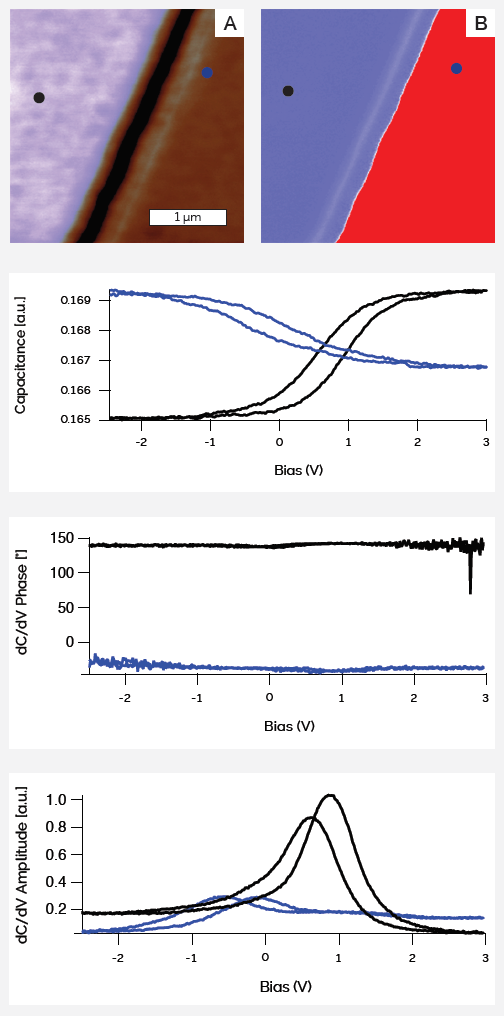
Figure 8. a) dC/dV amplitude image, b) dC/dV phase image, and (below images) Capacitance-voltage (C-V) spectra of two sides of a p-n junction of an SRAM sample, showing the different slopes of p-type (black curve) and n-type doping (blue curve). We can also see the phase and amplitude as a function of bias.
A reference sample with a known doping concentration must be employed for quantitative SCM experiments. Data gathered on a dopant staircase test sample produced by Infineon Technology is displayed in Figure 9 to demonstrate how this type of experiment can be performed.4
This reference sample includes strips of increasing dopant levels with concentration varying from 4×10¹⁵ to 1×10²⁰ atoms/cm3. Both p-doped and n-doped regions have equivalent dopant concentration strips within a range of 50 µm.
As displayed in Figure 9, both dC/dV channels and capacitance demonstrate strong signals when the stripes of dopant concentrations are mapped but the two signals respond differently.
The dC/dV amplitude is noted to be linear only for a subset of dopant concentrations, while the capacitance response is linear across the complete range of dopant concentrations for both p-doped and n-doped regions.
In combination with the research by Amster et al., these results show that a capacitance signal and an Infineon Technology reference sample can be utilized to measure the doping levels of unknown samples, so long as compensation for drift and stray capacitance are considered in the experimental design.5
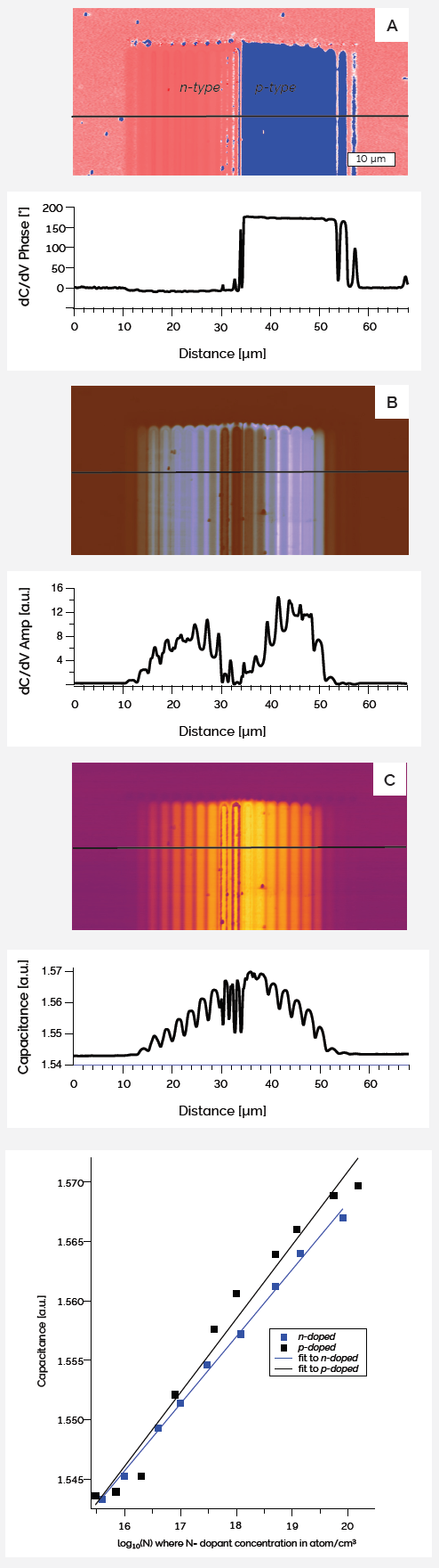
Figure 9. Infineon Technology dopant staircase reference sample. Images of a) dC/dV phase, b) dC/dV amplitude, and c) capacitance are shown as the sample was imaged at a sample bias of zero volts. Cross-sections of the same region are shown below the images.
It has traditionally been argued that dC/dV amplitude signal can be utilized to quantitatively measure concentrations of dopant, but this is highly bias dependent.
Figure 10 demonstrates that the dC/dV amplitude signal on the reference sample’s n-doped region becomes monotonic in relation to the doping level at a negative sample DC bias. At a positive sample bias, the dC/dV amplitude signal on the p-doped region is linear with the varying dopant level.
The response is not linear for both of the DC bias because of the interaction with the substrate on the lower range of the doping concentration (less than 1×10¹⁶ atoms/cm3).
The results outlined to demonstrate that when the correct DC bias is utilized and when dopant concentrations are higher than a particular level, the dC/dV amplitude signal can be employed for quantitative dopant level research.
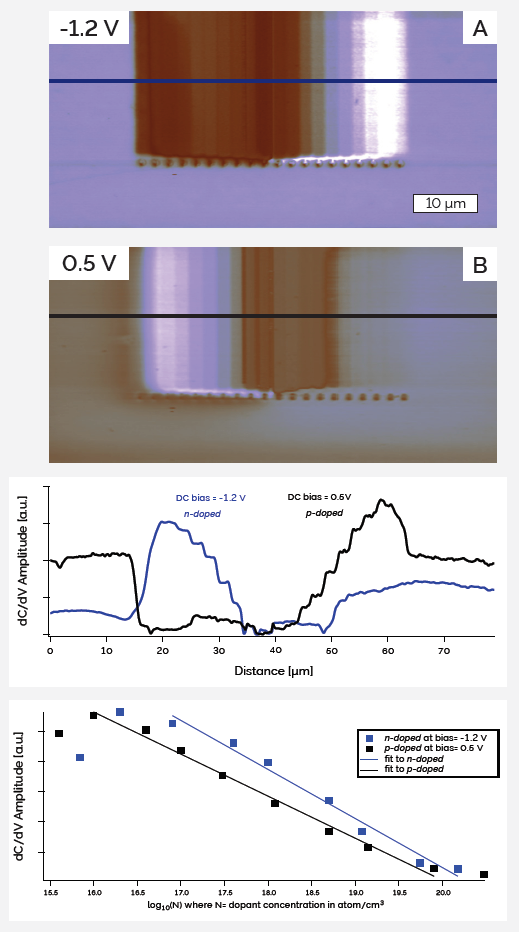
Figure 10. dC/dV amplitude images of the Infineon Technology sample were acquired at a) -1.2 V and b) 0.5 V DC bias. (Bottom) The linear relationship of the dC/dV amplitude signal with dopant concentration is observed to be strongly bias dependent.
Examples on Non-Semiconductor Materials
SCM can be a beneficial characterization technique for materials beyond traditional semiconductor samples. This section outlines how SCM can be applied in the measurement and analysis of 2D materials, carbon nanotubes, ferroelectrics, and batteries.
Copper indium di-sulfide (CuInS2) was imaged after being applied to silicon to find out whether the reflected microwave signal (capacitance image) could identify the range of thicknesses in 2D materials.
Changing the material’s impedance beneath the probe tip will disrupt the microwave signal and will result in a change in the reflected signal, which will provide contrast in the capacitance channel.
Figure 11 demonstrates a distinct correlation between the thickness of the material deposited onto the substrate and the capacitance signal. This outcome shows good potential for the utilization of SCM to efficiently identify the thickness of exfoliated 2D materials.
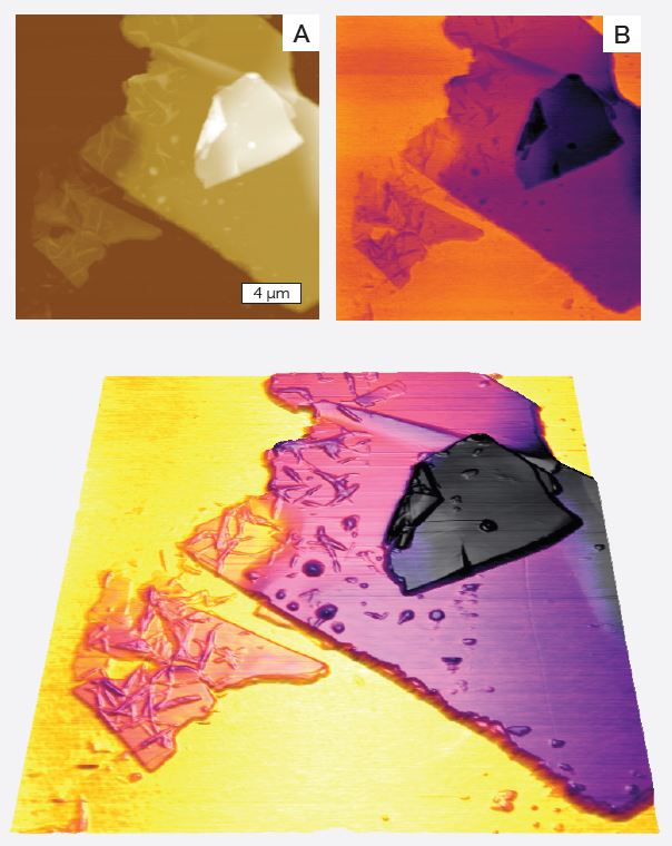
Figure 11. CuInS2 on silicon a) topography b) capacitance c) capacitance overlaid on topography. Image Credit: Sample courtesy of M. Cheng and Prof. V. Dravid of Northwestern University.
The SCM method can also be used to analyze any non-linear response in 2D materials. Molybdenum disulfide (MoS2) is a material employed in electronic applications and identifying how its features are reliant on thickness is crucial for accurate device production.
Variations in the dC/dV amplitude signal were noted when the MoS2 sheets were imaged (Figure 12). The change in the bandgap and the work function of the material with different material thickness was likely the cause of these changes.
The addition to the number of material layers did not demonstrate a linear increase in dC/dV amplitude signal, as such the behavior was non-linear. Due to the capacitance channel, SCM was shown to be a beneficial method for the evaluation of non-linear characteristics of 2D materials, even without the presence of oxide in this sample type.
The investigation and development of unique materials for energy storage is a crucial area of research where SCM data could be beneficial. Here, a battery’s test electrode (Figure 13) was imaged.
Providing information about electron conduction, a distinct contrast was seen in the capacitance channel at grain boundaries and on individual grains. The variations in capacitance contrast on the surface are distinct from the surface topography.
This information could be correlated with electrochemical strain microscopy and conductive AFM to understand functional and structural characteristics further.
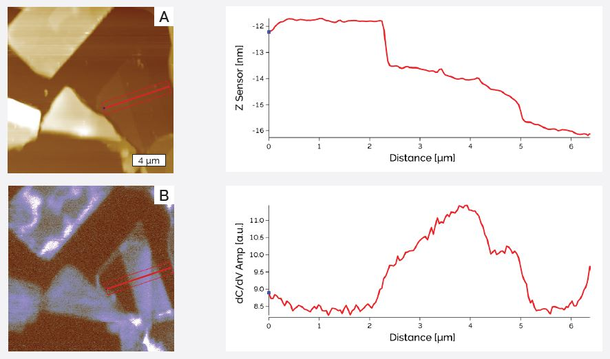
Figure 12. MoS2 sample a) height b) dC/dV Amplitude and c) cross-sections of topography and dC/dV amplitude images of the same area. Topography and the dC/dV amplitude signal do not show linear correlation: the number of material layers does not correspond to a linear increase in dC/dV amplitude signal. Image Credit: Sample is courtesy of A. Kis at EPFL.
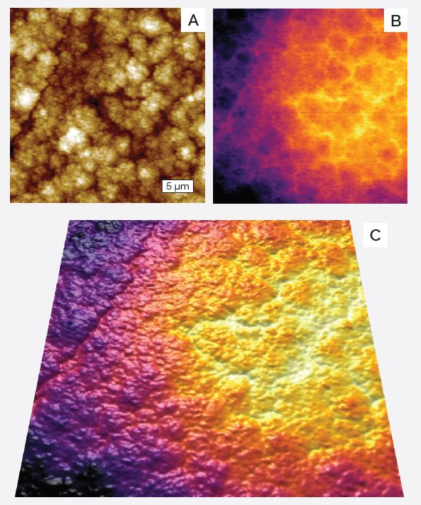
Figure 13. Test electrode of a battery. a) topography, b) capacitance, c) capacitance overlaid onto topography.
Quantum dots can be beneficial for applications in quantum computing and materials emulation which means measuring their electronic features is critical. Grown on a Si substrate, a sample of polycrystalline Si quantum dots was imaged (Figure 14) and the result is shown as a 3D demonstration of capacitance overlaid onto the topography. Contrast variation was noted between separate quantum dots along with the empty surface devoid of dots.
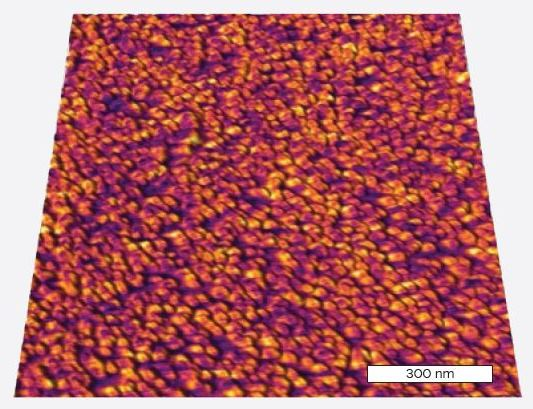
Figure 14. Polycrystalline quantum dots on silicon. 3D rendition of capacitance signal overlaid on topography.
The electrical performance and features of carbon nanotubes make them a potential interest for analysis as an additive or material for battery research. A carbon nanotube (CNT) sample was imaged using SCM which spanned two electrodes (Figure 15).
The CNT was semiconducting in behavior and structure and demonstrated a distinct signal in both the dC/dV channels and capacitance. To acquire the image, one electrode was left floating and the 90 kHz modulation bias was applied to the other electrode (as displayed in Figure 15C).
The dC/dV Amplitude signal shows that the Si sample substrate has a higher doping concentration than the CNT. Close to the electrode, there is also an interesting behavior that arises.
The CNT appears to have a higher conductivity close to the electrode than when it is farther away. It is likely that the CNT is ‘doped’ by the deposition of the electrode when it is near.
The dC/dV phase channel exhibits a strong contrast of almost 180°. In the capacitance signal, some noise is observed which could be a result of the very weak signal created by such a small nanowire.
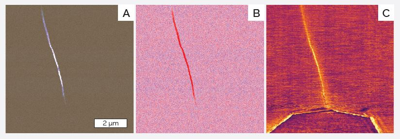
Figure 15. CNT spanning two electrodes. a) dC/dV Amplitude, b) dC/dV phase, and c) capacitance. Overlay of dC/dV amplitude on topography. One electrode can be seen at the bottom of the image but the other is out of the scan area. Image Credit: Sample courtesy of Laurel Anderson and Philip Kim, SEAS, Harvard, University.
In Figure 16, CNT was imaged utilizing a metal-coated silicon probe after being deposited on an insulating substrate. The high resolution of the image is due to the highly sensitive SCM module. A 23 nm resolution is noted by the cross-section of the CNT in the capacitance.
Lastly, SCM can additionally be employed to analyze piezoelectric samples.7 As displayed in Figure 17, the PZT nanoparticles appear identical in the height image but have strong differentiation in the SCM images.
In the dC/dV amplitude image, the fine domain structure can also be observed. The dC/dV spectra demonstrate a significant hysteresis loop, suggesting piezoelectric behavior.8 SCM can be a complementary technique in the investigation of piezoelectric and ferroelectric materials.9
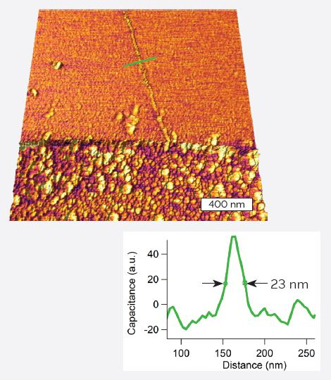
Figure 16. CNT on an insulating substrate. Capacitance data overlaid on 3D topography. Image Credit: Sample is courtesy of B. Wilson and J. Tresback, Harvard Center for Nanoscale Systems.
Conclusion
The updated SCM module is of special interest for the investigation of non-linear electronic materials and has significant potential for the qualitative measurement of conductors and insulators.
This article presented examples of SCM applications in semiconducting materials, energy storage, quantum dots, ferroelectric and 2D materials, and nanowires along with showing the high imaging rate, unrivaled sensitivity, and high resolution of the module.
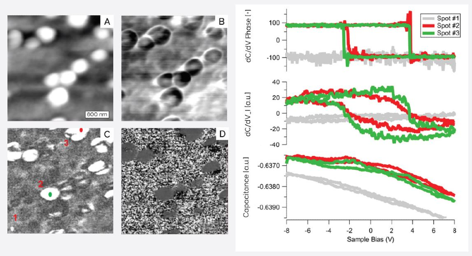
Figure 17. SCM images, a) Height, b) Capacitance, c) dC/dV Amplitude, and d) dC/dV Phase and dC/dV spectra on PZT nanoparticles showing the hysteresis loop of the ferroelectricity.
References and Further Reading
- Matey, JR; J Blanc (1985). “Scanning Capacitance Microscopy”. Journal of Applied Physics. 57 (5): 1437–1444; C.C. Williams (1999). “Two-dimensional dopant profiling by scanning capacitance microscopy”. Annual Review of Materials Research. 29: 471–504.
- Ganesh Prasad Srivastava, Vijay Laxmi Gupta, Microwave Devices and Circuit Design, pp.29-31, PHI Learning, 2006.
- Asylum RMN probes. https://afmprobes.asylumresearch.com/catalogsearch/result/?q=rmn&cat=
- T. Schweinböck and S. Hommel, Quantitative Scanning Microwave Microscopy: A calibration flow, Microelectronics Reliability, 2014, 54(9–10), 2070.
- Oskar Amster et.al., Microelectronics Reliability 76–77 (2017) 214–217.
- J. Smoliner, B. Basnar, S. Golka, and E. Gornik, Appl. Phys. Lett. 79, 3182 (2001).
- Ching-Chich Leu et.al., Appl. Phys. Lett. 82, 3493 (2003).
- Daehee Seol, Bora Kim, Yunseok Kim, Current Applied Physics 17(5) (2017).
- Suraj Cheema et.al, Ultrathin-enhanced ferroelectricity directly on silicon, Nature 23 April (2020).

This information has been sourced, reviewed and adapted from materials provided by Asylum Research - An Oxford Instruments Company.
For more information on this source, please visit Asylum Research - An Oxford Instruments Company.