Electron beams are ideal for probing sample surfaces beyond visible light and supplying powerful magnifications which are many orders of magnitude higher than that of optical microscopy.
Resolving power is not the final word when working with resolutions of nanometer (nm) and sub-nm proportions. This is partly because, when molecular-scale imaging solutions are involved, researchers have so many options.
If a user wanted to evaluate both the topographical and morphological properties of a metal surface, then electron microscopy would be able to supply detailed insights into grain size, phase structure, etc.
Scanning probe microscopy (SPM) can provide more detailed insights into the three-dimensional surface structures, even if a metal surface is topographically uniform at the nanoscale, so which method is best for your application?
Today, physical scanning probes and electron beams are usually utilized together for comprehensive sample analysis, so the user would not have to choose between them.

Image Credit: Platypus Technologies, LLC
AFM: The Basics
The most popular microscopic technique, which is based on scanning probe technology, is probably atomic force microscopy (AFM). By resolving even the subtlest topographical variations of highly smooth surfaces, it can complement methods such as scanning or transmission electron microscopy (SEM/TEM).
AFM can also resolve a range of compositional qualities such as magnetism, elasticity, adhesiveness, stiffness, etc. Specialized probe tips and precision-engineered substrates that promote high signal-to-noise ratios are needed to achieve this.
One quick example is that AFM has been identified as a good technique for assessing the quality of self-assembled monolayer (SAM) printing on functionalized metallic surfaces.
These unique, organic molecules are formed on surfaces spontaneously via adsorption based on intermolecular and molecular substrates, known as molecule interactions.
Subsequently, AFM can evaluate printing parameters and identify pattern errors within a single molecule. Yet, this exceptional level of precision requires ultra-flat substrates – usually metallic surfaces like gold.
Template-Stripped Metallic Surfaces
Flat means topographically uniform at the atomic scale in the context of AFM. This is not an easy quality to obtain using conventional manufacturing techniques such as flame annealing or epitaxy.
Although they can supply a good level of flatness, this is limited to flakes that have surface areas that are smaller than two micrometers (µm2), representing a prohibitively small substrate. The majority of applications need larger metallic surfaces.
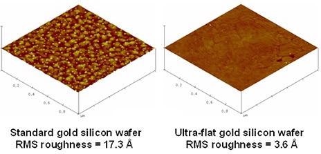
Image Credit: Platypus Technologies, LLC
One novel method which is utilized to replicate the natural flatness of mica glass or polished silica in a metallic surface like gold is template-stripping. The user is able to deposit an adhesive intermediate on a glass/silicon chip and coat the template with a uniform gold thin film.
The large area Angstrom-scale uniformity of the underlying substrates translates through to the metallic surface to produce a highly functional gold substrate with pristine design topographies.
This allows researchers to attain the ultra-high resolution that is needed for characterizing materials at the atomic range with negligible interference from substrate inhomogeneities or undesirable surface-tip interactions.
In addition to assessing SAMs, template-stripped metallic surfaces have proven ideal in DNA origami, single-molecule imaging, 2D materials characterization and a number of other applications.

This information has been sourced, reviewed and adapted from materials provided by Platypus Technologies, LLC.
For more information on this source, please visit Platypus Technologies, LLC.