One growing engineering paradigm which allows technicians to create a large variety of intricate, prototypical parts is additive manufacturing (AM). Small-scale patterned electrodes for scientific micro-electromechanical systems (MEMS) are among these.
The Basics of Printed Electrodes
Typically, integrated circuitry for sensing elements is produced via selective sublimation by utilizing a photoresist that is exposed to X-ray or electron beams. There are numerous parts to the conventional printing process, and these include pre-treatment with photo-resistant solvents and ex-situ modification (i.e., chemical etching).
For patterned electrodes, which are intended for chemical or biosensing sensor chips where negligible contamination is required to ensure quality of results, this can be a challenge. The surface morphology of patterned electrodes can also have a demonstrable effect on electrical performance, which influences detection efficiency.
Subsequently, nanopatterned electrodes that are generated via deposition are an attractive prospect for electrochemical assays, bioMEMS, and other extremely high-sensitivity electrical platforms. They can now be produced by utilizing a raft of AM methods, from e-beam evaporation to screen printing.
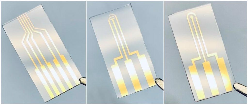
Image Credit: Platypus Technologies, LLC
E-Beam Evaporation for Patterned Electrodes
One of the favored techniques for generating highly conductive three-dimensional patterns on functional substrates with high lateral fidelity and low surface roughness is electron beam physical vapor deposition (EBPVD).
EBPVD can yield high-sensitivity patterned electrodes which have low roughness down to the nanoscale by utilizing ultra-clean glass substrates with a titanium adhesion layer and a completely pure (<99.999%) gold anode and deposition rates which are tightly controlled.
The optical transparency of the glass substrate allows the easy visual sensing of the conductive gold layer, which is cleanly and strongly adhered to the substrate by the chemically-pure titanium intermediary. This enables a number of advantages for in situ visualizations of experimentation via spectroscopy or microscopy.
Platypus Technologies have fine-tuned their e-beam processing capabilities to ensure outstanding repeatability, which has allowed them to launch a proprietary line of research-grade gold patterned electrodes.
These electrodes include:
- A disk electrode which is intended for cyclic voltammetry or electrochemical impedance spectroscopy (EIS)
- A resistivity electrode which is a 5-probe microelectrode, perfect for calculating sheet impedance, resistance, or conductivity of numerous materials
- A 3-probe electrode is made for bio- and chemical sensor R&D.
Patterned Electrodes from Platypus Technologies
Platypus Technologies provide a number of off-the-shelf solutions for scientific imaging, but the Platypus Tech specialty is custom coating for proprietary applications.

This information has been sourced, reviewed and adapted from materials provided by Platypus Technologies, LLC.
For more information on this source, please visit Platypus Technologies, LLC.