Oct 1 2021
Nanowires and nanofins have a large surface-to-volume ratio, and they greatly react with the environment. GaN nanostructures also react with major air constituents, and under controlled environments can be used for various applications in areas like environmental sensing, photocatalysis, and light-emitting diodes.
GaN (Gallium nitride) Nanowires (NW) have garnered interest in the last years as they can be created with high crystal quality. Moreover, GaN NWs show good optical properties like strong luminescence upon electrical or optical excitation; probing changes of the luminescence under controlled environmental conditions is a promising pathway to understand the underlying mechanisms.
The GaN surfaces react with the environment, and knowledge of the phenomenon could trigger advancements in highly relevant fields like sensing, photocatalysis, or the improvement of nanowire (NW) light-emitting diodes (LEDs).
Scientists analyzed the influence of GaN NW geometry, different gaseous atmospheres, the pH value, and electrical fields in aqueous solutions on the intensity of the photoluminescence (PL) response and the NW stability. Earlier research shows that anions that accumulate at the NW surface enhance non-radiative recombination and, therefore, reduce the PL intensity.
The current paper discusses the luminescence behavior and the role of surface-related processes of GaN NWs under different atmospheres with a focus on the main constituents of ambient air, nitrogen (N2), oxygen (O2), and water (H2O) vapor.
This is in turn combined with the analyzes of the effects of pre-treatments, which can have a significant influence on several surface properties of c- and m-planes of GaN, including the magnitude of the surface band bending (SBB). Various oxide shells are also tested on their capability to stabilize the PL emission of GaN NWs and elucidate the effect of several common solvents on the PL intensity evolution.
Experimental Details
The GaN Nanostructures (GaN NS) analyzed were grown through plasma-assisted molecular beam epitaxy (MBE) in a selective area growth mode.
The GaN NWs were grown on n-type Si (111) substrates (iron-compensated Ga-polar GaN templates) under N-rich conditions at a substrate temperature of 875 °C (950 °C) with a Ga flux of 5.7 (4.6) 10−7 mbar beam equivalent pressure (BEP) and an N2 flux of 0.363 sccm with an RF plasma power of 425 W for 90 minutes at a background pressure of about 10−0 mbar. The Nano Wires had a uniform shape and similar dimensions.
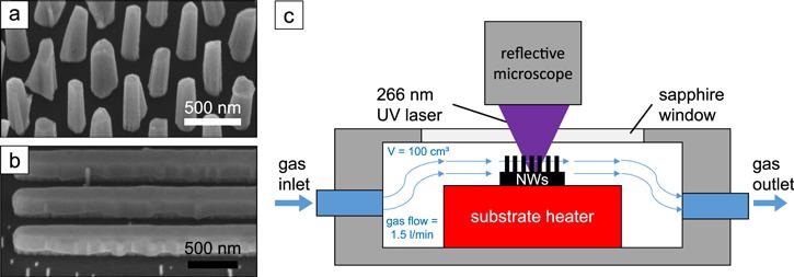
Figure 1. (a) SEM image of GaN NWs on a Si substrate and (b) GaN nanofins on an AlN substrate in 45°-tilted view. (c) Sketch of the measurement chamber with gas flow and resistive heater. Image Credit: Kraut et al., 2021
Three batches of NW arrays were grown on Si to examine the influence of common cleaning treatments of the GaN NW surface on their sensitivity to the environment. NWs labeled “oxidized” are exposed to an oxygen plasma with an RF power of 400 W and an O2 flow of 0.6 sccm at a temperature of 600 °C in an ultra-high vacuum chamber for 10 minutes.
The optical investigation and light exposure of the GaN NW surfaces during interaction with their environments was understood by above-band gap light excitation with a quadrupled Nd:YAG laser with a wavelength of 266 nm in continuous-wave operation.
The excitation intensity was measured by placing a power sensor instead of a sample into the optical path. In ambient air, a 40× UV-enhanced High-Power MicroSpot objective with a working distance of 1 mm and a resulting laser spot size of roughly 2 μm was used.
Wet environment measurements were taken by bubbling the respective gases through deionized (DI) H2O until a relative humidity of 100% was reached, while in liquid environment measurements, the sample was mounted into a Petri dish filled with the respective fluid.
Results and Discussion
PL Intensity in Air
The complexity of the photoluminescence (PL) in response to GaN NWs in the air is depicted in Figure 2(a). In the saturation regime, the speed of the PL enhancement has to be limited by the speed of adsorption or desorption of molecules from the environment to or from the NW surface.
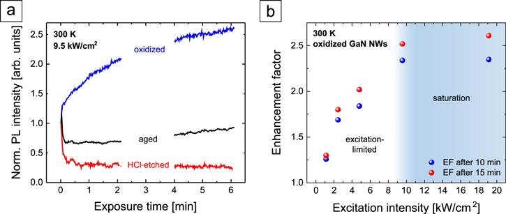
Figure 2. (a) NBE PL intensity evolution of GaN NWs in ambient air (T = 300 K) normalized to the initial value. (b) Enhancement factor of the PL intensity of oxidized GaN NWs after 10 and 15 min under UV light exposure as a function of the excitation intensity. Image Credit: Kraut et al., 2021
PL Intensity in Controlled Atmospheres
To understand the interactions at the NW surface, a more accurate controlled experimental environment is needed. Figure 3 shows the normalized saturated PL intensity under continuous UV illumination with an excitation intensity of 18 kW cm−2 for HCl-etched and oxidized NWs under varied atmospheres and for different temperatures. The PL intensity measured in dry N2 is used as the reference value for normalization.
In humid SA, the PL intensity of the oxidized GaN NWs decreases to 60% of the dry N2 level and 15% for the HCl-etched NWs within 1 min. And as a final step, when the flow-chamber is purged with dry N2, both samples increase their PL emission back to the initial level within the measurement error, which underlines the reversible nature of the observed effects.
In SA and N2 atmospheres, the values obtained for dry and humid environments are similar and while switching back to first wet and later dry N2 decreases the luminescence to about 3 and 1.5 times the initial value, respectively.
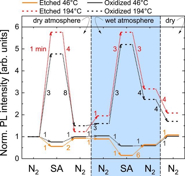
Figure 3. Variation of the stabilized NBE PL intensity of oxidized and HCl-etched GaN NWs in different atmospheres under continuous illumination. The numbers next to the dotted arrows indicate the typical transition time from one steady-state to the other. An excitation intensity of 18 kW cm−2 has been used. The given Teff was determined by the evaluation of the NBE peak position of GaN. Image Credit: Kraut et al., 2021.
The researchers conclude that oxygen alone can form two fundamentally different interacting states at the NW surface.
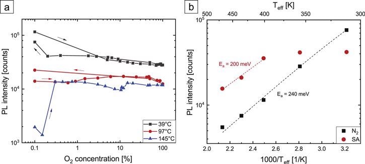
Figure 4. (a) PL intensity of HCl-etched GaN NWs in dry atmospheres as a function of O2 concentration in N2 background for several Teff. (b) Arrhenius plot of the temperature dependence of the PL intensity in dry N2 and SA atmospheres. For all measurements, an excitation density of 18 kW cm−2 was used. Dashed lines are Arrhenius fits. Image Credit: Kraut et al., 2021
PL Intensity Evolution After Illumination Onset
The PL intensity evolution immediately after the UV excitation onset probes the light-induced changes of the surface properties in a given ambient. The PL intensity of the oxidized GaN NWs in dry N2 increases within 1 min to 140% of the initial value, whereas in humid N2 it reaches only 120%.
The HCl-etched GaN NWs show almost no change in the PL intensity in dry N2, but a pronounced quenching of the PL signal to 50% of the initial intensity in humid N2. The equivalent measurements in dry and humid SA.
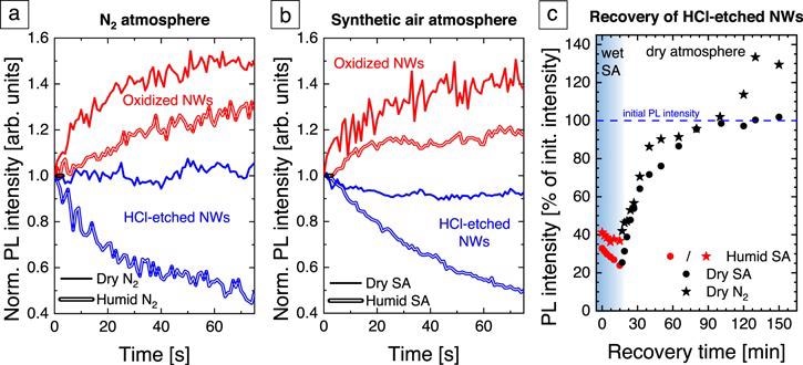
Figure 5. Normalized PL intensity evolution of oxidized (red) and HCl-etched (blue) GaN NWs after UV laser illumination onset with an excitation intensity of 18 kW cm−2 (a) in N2 (b) in SA. The solid (doubled) lines represent measurements in a dry (humid) atmosphere. (c) PL intensity recovery of HCl-etched GaN NWs in different atmospheres. The red symbols show the PL intensity after switching the laser illumination in humid SA. The black dots (stars) show the recovery behavior in dry SA (N2). The data are normalized to the initial PL intensity in dry SA before the quenching procedure. Image Credit: Kraut et al., 2021.
Combined PL and Electrical Measurements
Complementary electrical measurements of GaN NFs can provide further insight into the underlying mechanisms. Figure 6(a) depicts the electrical current through GaN NFs under illumination with 266 nm laser light and the simultaneously measured NBE PL in varied dry atmospheres at room temperature.
Under illumination, the total current (dark and photocurrent) decreases to 88% and recovers to 95%. A possible explanation lies in the location of photo-excitation within the GaN NF, which mainly takes place in the surface region, while the majority of the dark current contribution is through the conductive channel in the center of the NF.
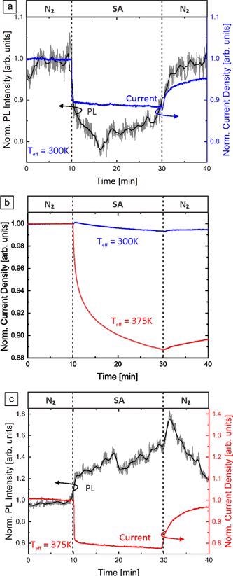
Figure 6. Normalized NBE PL intensity and normalized current density of GaN NFs on an AlN template under illumination with 266 nm light at (a) 300 K and (c) 375 K. The atmosphere was changed from dry N2 to dry SA and back under constant applied voltage (1 V) and excitation intensity (18 kW cm−2). (b) The normalized current density of GaN NFs at 300 and 375 K in the dark. Due to the sake of argument (c) is discussed later in the text. Image Credit: Kraut et al., 2021
Generally, changes in PL intensity of NSs under constant excitation originate in changes in the ratio of radiative to non-radiative charge carrier recombination. This is either caused by the creation or passivation of non-radiative recombination channels, for example, unsaturated surface states, or by changing the amount of radiative recombination through spatial separation of electrons and holes, for instance, due to SBB.
Figure 7(b) summarizes the CPD and SPV results in a schematic drawing of the GaN NS SBB in SA and N2 atmosphere. In the dark, the SBB in SA is higher than in N2. This difference increases upon above bandgap illumination as the SBB reduction due to the light is more pronounced in SA compared to N2.
This matches well with the increased sensitivity of the current to changing the atmosphere under illumination compared to in the dark (Figure 6): the higher reduction of the SBB under illumination leads to a stronger shrinking of the conductive channel within the NF, which increases the electrical resistivity to a greater extend.
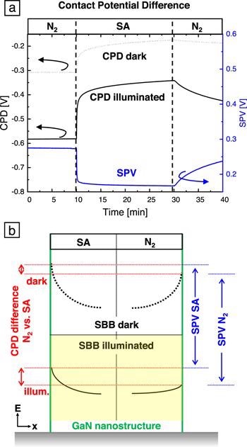
Figure 7. CPD of an m-plane bulk GaN plate in the dark and under 340 nm illumination with an excitation intensity of 6 mW cm−2. The atmosphere was changed from dry N2 to dry SA and back. (b) Schematic drawing of the band bending at a GaN NS surface (green line) in SA (left) and N2 (right) atmosphere at room temperature. The dashed/solid black lines represent the SBB in the dark/under illumination. The red lines illustrate the CPD differences between SA and N2 atmosphere in the dark (upper part) and under illumination (lower part). The corresponding SPV in SA and N2 are indicated in blue. Image Credit: Kraut et al., 2021.
PL Response in Liquid Environments
Figure 8 depicts the PL response of HCl-etched GaN NWs in various liquids on a logarithmic scale. The various magnitude of the PL response in different liquid environments opens a possibility to use GaN NWs to optically identify impurity molecules for, for example, H2O quality control applications.
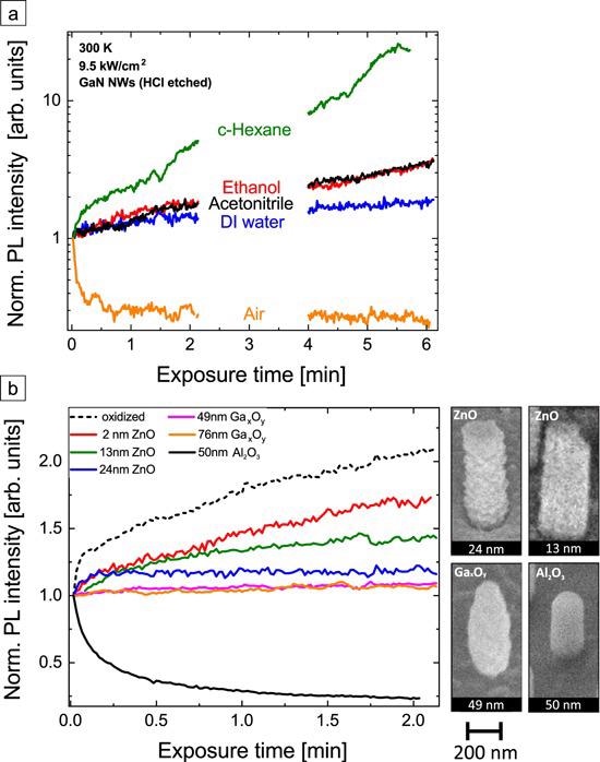
Figure 8. (a) Normalized PL intensity evolution of HCl-etched GaN NWs after UV laser illumination onset with an excitation intensity of 9.5 kW cm−2 in the air (orange), DI H2O (blue), acetonitrile (black), ethanol (red), and cyclohexane (green). The PL intensity axis is shown with a logarithmic scale. (b) Normalized PL intensity of GaN NWs with several shells at an excitation intensity of 9.5 kW cm−2 in ambient conditions. For comparison, oxidized NWs are also shown. ZnO and Gax Oy shells are MBE-grown, the 50 nm Al2O3 was deposited by ALD. SEM images in a 45° tilted view of exemplary NWs with different shells are depicted at the right of the graph. Image Credit: Kraut et al., 2021.
GaN-Metal Oxide Core–Shell NWs
The MBE-coated samples (ZnO, Gax Oy) indicate an intensity increase, but the amplitude differs significantly. While the PL signal of the GaN NBE of the oxidized NWs more than doubled within 2 min, for the thickest Gax Oy shell it increases only by 6%.
The absolute PL intensities (table S5, SI) of the GaN-ZnO core-shell NWs decrease by a factor of almost 25 from the thinnest to the thickest shell due to absorption of the excitation laser in the ZnO. Further, the sample with an Al2O3 shell exhibits the highest PL signal and is at the same time the only one exhibiting a decreasing PL intensity over-illumination time.
Conclusion
Knowledge of the influence of the environment on the optical and electrical properties of nanostructures (NSs) is a matter of high technological importance and scientific interest. The research carried out an extensive and systematic investigation of some major external contributions manipulating the photoluminescence (PL) intensity and the electrical resistance of GaN nanowires (NWs) and GaN nanofins (NFs) on several substrates.
One major finding is that both H2O and oxygen show an ambivalent influence with either quenching or enhancing effect, depending on the sample temperature. While for the PL-influencing adsorption of H2O the ultraviolet (UV) illumination plays a key role, the surface reactions related to oxygen also take place in the dark.
The results highlight the importance of controlled environmental conditions, surface treatments, and passivation technologies to ensure reliable experimental results and for boosting device performances.
Journal Reference:
Kraut, M., Pantle, F., Wörle, S., Sirotti, E., Zeidler, A., Eckmann, F. and Stutzmann, M., (2021) Influence of environmental conditions and surface treatments on the photoluminescence properties of GaN nanowires and nanofins. Nanotechnology, 32(49), p.495703. Available at: https://iopscience.iop.org/article/10.1088/1361-6528/ac1dd1#nanoac1dd1s5
References and Further Reading
- Wallys, J., et al. (2012) Bias-enhanced optical pH response of group III-nitride nanowires. Nano Letters, 12, pp. 6180–6186. doi.org/10.1021/nl303021v.
- Wright, J., et al. (2009) Hydrogen sensing with Pt-functionalized GaN nanowires. Sensors and Actuators B: Chemical, 140, pp. 196–199. doi.org/10.1016/j.snb.2009.04.009.
- Aluri, G. S., et al. (2011) Highly selective GaN-nanowire/TiO2-nanocluster hybrid sensors for detection of benzene and related environment pollutants. Nanotechnology, 22, pp. 295–503. doi.org/10.1088/0957-4484/22/29/295503.
- Hersee, S., et al. (2009) GaN nanowire light emitting diodes based on templated and scalable nanowire growth process. Electronics Letters, 45, pp. 75–76. doi.org/10.1049/el:20092391.
- Lee, S.-K., et al. (2007) High-brightness gallium nitride nanowire UV-blue light emitting diodes. Philosophical Magazine, 87, pp. 2105–2115. doi.org/10.1080/14786430701199648.
- Wang, D., et al. (2011) Wafer-level photocatalytic water splitting on GaN nanowire arrays grown by molecular beam epitaxy. Nano Letters, 11, pp. 2353–2357. doi.org/10.1021/nl2006802.
- Jung, H. S., et al. (2008) Photocatalysis using GaN nanowires. ACS Nano, 2, pp. 637–642. doi.org/10.1021/nn700320y.
- Chen, C.-P., et al. (2011) Ultrasensitive in situ label-free DNA detection using a GaN nanowire-based extended-gate field-effect-transistor sensor. Analytical Chemistry, 83, pp. 1938–1943. doi.org/10.1021/ac102489y.
- Asadnia, M., et al. (2016) Mercury (II) selective sensors based on AlGaN/GaN transistors. Analytica Chimica Acta, 943, pp. 1–7. doi.org/10.1016/j.aca.2016.08.045.
- Yu, X., et al. (2008) Wireless hydrogen sensor network using AlGaN/GaN high electron mobility transistor differential diode sensors. Sensors Actuators B, 135, pp. 188–194. doi.org/10.1016/j.snb.2008.08.005.
- Auzelle, T., et al. (2021) External control of GaN band bending using phosphonate self-assembled monolayers. ACS Applied Materials & Interfaces, 13, pp. 4626–4635. doi.org/10.1021/acsami.0c17519.
- Foussekis, M., et al. (2009) Photoadsorption and photodesorption for GaN. Applied Physics Letters, 94, p. 162116. doi.org/10.1063/1.3122934.
- Auzelle, T., et al. (2021) Enhanced radiative efficiency in GaN nanowires grown on sputtered TiNx: effects of surface electric fields. ACS Photonics, 13, pp. 4626–4635. doi.org/10.1021/acsphotonics.1c00224.
- Winnerl, A., et al. (2017) Photo-induced changes of the surface band bending in GaN: influence of growth technique, doping and polarity. Journal of Applied Physics, 121, pp. 205–307. doi.org/10.1063/1.4983846.
- Teubert, J., et al. (2011) GaN nanodiscs embedded in nanowires as optochemical transducers. Nanotechnology, 22, pp. 275–505.
- Maier, K., et al. (2017) Photoluminescence probing of complex H2O adsorption on InGaN/GaN nanowires. Nano Letters, 17, pp. 615–621. doi.org/10.1021/acs.nanolett.6b03299.
- Maier, K., et al. (2018) Photoluminescence detection of surface oxidation processes on InGaN/GaN nanowire arrays. ACS Sensors, 3, pp. 2254–2260. doi.org/10.1021/acssensors.8b00417.
- Hetzl, M., et al. (2018) A systematic investigation of radiative recombination in GaN nanowires: The influence of nanowire geometry and environmental conditions. Journal of Applied Physics, 124, p. 035704. doi.org/10.1063/1.5038802.
- Kraut, M., et al. (2019) Photo-induced selective etching of GaN nanowires in water. Nanoscale, 11, pp. 7967–7975. doi.org/10.1039/C8NR10021G.
- Garcia, M. A., et al. (2006) Surface oxide relationships to band bending in GaN. Applied Physics Letters, 88, p. 013506. doi.org/10.1063/1.2158701.
- Auzelle, T., et al. (2019) Electronic properties of air-exposed GaN (11-00) and (0001) surfaces after several device processing compatible cleaning steps. Applied Surface Science, 495, p. 143514. doi.org/10.1016/j.apsusc.2019.07.256.
- Hetzl, M., et al. (2016) Reprint of: GaN nanowires on diamond. Materials Science in Semiconductor Processing, 55, pp. 32–45. doi.org/10.1016/j.mssp.2016.03.013.
- Pantle, F., et al. (2021) Selective area growth of GaN nanowires and nanofins by molecular beam epitaxy on heteroepitaxial diamond (001) substrates. Nanoscale Advances, 3, pp. 3835–3845. doi.org/10.1039/D1NA00221J.
- Schuster, F., et al. (2015) Position-controlled growth of GaN nanowires and nanotubes on diamond by molecular beam epitaxy. Nano Letters, 15, pp. 1773–1779. doi.org/10.1021/nl504446r.
- Hetzl, M., et al. (2017) Polarity control of heteroepitaxial GaN nanowires on diamond. Nano Letters, 17, pp. 3582–3590. doi.org/10.1021/acs.nanolett.7b00741.
- Winnerl, J., et al. (2019) Selectively grown GaN nanowalls and nanogrids for photocatalysis: growth and optical properties. Nanoscale, 11, pp. 4578–4584. doi.org/10.1039/C8NR09094G.
- Bertness, K. A., et al. (2008) Mechanism for spontaneous growth of GaN nanowires with molecular beam epitaxy. Journal of Crystal Growth, 310, pp. 3154–3158. doi.org/10.1016/j.jcrysgro.2008.03.033.
- Furtmayr, F., et al. (2008) Nucleation and growth of GaN nanorods on Si (111) surfaces by plasma-assisted molecular beam epitaxy - The influence of Si-and Mg-doping. Journal of Applied Physics, 104, p. 034309. doi.org/10.1063/1.2953087.
- Calarco, R., et al. (2005) Size-dependent photoconductivity in MBE-grown GaN-nanowires. Nano Letters, 5, pp. 981–984. doi.org/10.1021/nl0500306.
- Varshni Y P (1967) Temperature dependence of the energy gap in semiconductors. Physica, 34, pp. 149–154. doi.org/10.1016/0031-8914(67)90062-6.
- Prall, C., et al. (2014) Photoluminescence from GaN layers at high temperatures as a candidate for in situ monitoring in MOVPE. Journal of Crystal Growth, 397, pp. 24–28. doi.org/10.1016/j.jcrysgro.2014.04.001.
- Maier, K., et al. (2020) Luminescence probing of surface adsorption processes using InGaN/GaN nanowire heterostructure arrays. In: Semiconductor Gas Sensors (Woodhead Publishing Series in Electronic and Optical Materials), 2nd edn, pp. 239–270. doi.org/10.1016/B978-0-08-102559-8.00008-2.
- Fairchild, P W & Lee, E K (1978) Relative quantum yields of O (1D) in ozone photolysis in the region between 250 and 300 nm. Chemical Physics Letters, 60, pp. 36–39. doi.org/10.1016/0009-2614(78)85704-2.
- Nosaka, Y & Nosaka, A Y (2017) Generation and detection of reactive oxygen species in photocatalysis. Chemical Reviews, 117, pp. 11302–11336. doi.org/10.1021/acs.chemrev.7b00161.
- Smith, A. R., et al. (1998) Determination of wurtzite GaN lattice polarity based on surface reconstruction. Applied Physics Letters, 72, pp. 2114–2116. doi.org/10.1063/1.121293.
- Eickhoff, M., et al. (2001) Wetting Behaviour of GaN Surfaces with Ga-or N-Face Polarity. Physica Status Solidi b, 228, pp. 519–522. doi.org/10.1002/1521-3951(200111)228:2<519::AID-PSSB519>3.0.CO;2-A.
- Pfüller, C., et al. (2010) Unpinning the Fermi level of GaN nanowires by ultraviolet radiation. Physical Review B, 82, p. 045320. doi.org/10.1103/PhysRevB.82.045320.
- Calarco, R., et al. (2011) Surface-induced effects in GaN nanowires. Journal of Materials Research, 26, p. 2157. doi.org/10.1557/jmr.2011.211.
- Lefebvre, P., et al. (2012) Oxygen photo-adsorption related quenching of photoluminescence in group-III nitride nanocolumns. Superlattices and Microstructures, 52, pp. 165–171. doi.org/10.1016/j.spmi.2012.05.001.
- Cruz, S. C., et al. (2009) Crystallographic orientation dependence of dopant and impurity incorporation in GaN films grown by metalorganic chemical vapor deposition. Journal of Crystal Growth, 311, pp. 3817–3823. doi.org/10.1016/j.jcrysgro.2009.02.051.
- Sumiya, M., et al. (2020) Dynamic observation and theoretical analysis of initial O2 molecule adsorption on polar and m-plane surfaces of GaN. The Journal of Physical Chemistry C, 124, pp. 25282–25290. doi.org/10.1021/acs.jpcc.0c07151.
- Mehandru, R., et al. (2004) AlGaN/GaN HEMT based liquid sensors. Solid-State Electronics, 48, pp. 351–353. doi.org/10.1016/S0038-1101(03)00318-6.
- Stutzmann, M., et al. (2002) GaN-based heterostructures for sensor applications. Diamond and Related Materials, 11, pp. 886–891. doi.org/10.1016/S0925-9635(02)00026-2.
- Neuberger, R., et al. (2001) High-electron-mobility AlGaN/GaN transistors (HEMTs) for fluid monitoring applications. Physica Status Solidi a, 185, pp. 85–89. doi.org/10.1002/1521-396X(200105)185:1<85::AID-PSSA85>3.0.CO;2-U.
- Steinhoff, G., et al. (2003) pH response of GaN surfaces and its application for pH-sensitive field-effect transistors. Applied Physics Letters, 83, pp. 177–179. doi.org/10.1063/1.1589188.
- Zhang, Z & Yates, J T Jr (2012) Band bending in semiconductors: chemical and physical consequences at surfaces and interfaces. Chemical Reviews, 112, pp. 5520–5551. doi.org/10.1021/cr3000626.
- Quaranta, M., et al. (2013) A new method to measure oxygen solubility in organic solvents through optical oxygen sensing. Analyst, 138, pp. 6243–6245. doi.org/10.1039/C3AN36782G.
- Battino, R., et al. (1983) The solubility of oxygen and ozone in liquids. Journal of Physical and Chemical Reference Data, 12, pp. 163–178. doi.org/10.1063/1.555680.
- Shen, X., et al. (2009) Water adsorption on the GaN 1010 nonpolar surface. The Journal of Physical Chemistry C, 113, pp. 3365–3368. doi.org/10.1021/jp809499d.
- Esposto, M., et al. (2011) Electrical properties of atomic layer deposited aluminum oxide on gallium nitride. Applied Physics Letters, 99, p. 133503. doi.org/10.1063/1.3645616.
- Jia, Y., et al. (2017) Interface characterization of atomic layer deposited Al2O3 on m-plane GaN. Physica Status Solidi b, 254, p. 1600681. doi.org/10.1002/pssb.201600681.
- Dameron, A. A., et al. (2008) Gas diffusion barriers on polymers using multilayers fabricated by Al2O3 and rapid SiO2 atomic layer deposition. The Journal of Physical Chemistry C, 112, pp. 4573–4580. doi.org/10.1021/jp076866+.
- Henning, A., et al. (2021) Aluminum oxide at the monolayer limit via oxidant-free plasma-assisted atomic layer deposition on GaN. Advanced Functional Materials, 31, p. 2101441. doi.org/10.1002/adfm.202101441.
- Jackson, C. M., et al. (2017) Impact of surface treatment on interface states of ALD Al2O3/GaN interfaces. ECS Journal of Solid State Science and Technology, 6, p. 489. doi.org/10.1149/2.0041708jss.
- Zhang, Y., et al. (2020) Impact of Surface Treatments and Post-Deposition Annealing Upon Interfacial Property of ALD-Al2O3 on a-Plane GaN. IEEE Journal of the Electron Devices Society, 8, pp. 970–975. doi.org/10.1109/JEDS.2020.3020893.
- Horikawa, K., et al. (2020) Postdeposition annealing effect on the reliability of atomic-layer-deposited Al2O3 films on GaN. Journal of Vacuum Science & Technology B, 38, p. 062207. doi.org/10.1116/6.0000531.