Sponsored by Alemnis AGAug 16 2022Reviewed by Maria Osipova
Semiconductors are the foundation of modern-day technology, and improving their computing power is at the core of this dynamic industry.
However, the mechanical performance also matters: adhesion of functional layers, the strength of wire bonding, or scratch resistance of protective coatings are just a few examples that have wide-ranging implications on the development, quality control, and lifetime of a product.
As semiconductor technology is inherently small, traditional mechanical test methods are not suitable for assessing the mechanical properties of individual components.
Here, scanning electron microscopy (SEM) based micromechanical characterization techniques offer two considerable advantages: Firstly, providing accurate and unique correlative data thanks to in situ imaging and analytics, and secondly, offering a force and displacement resolution in the µN and pm range, respectively.
This article provides an overview of micromechanical testing applications in the semiconductor domain, with a focus on the highly versatile suite of testing equipment offered by Alemnis AG.
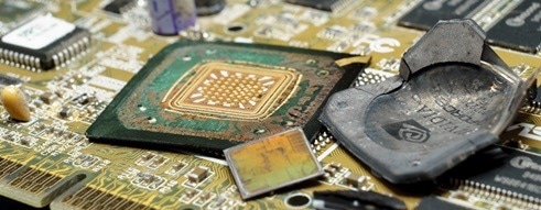
Figure 1. The reliability of semiconductor devices depends on numerous components: From substrates to films, from bonding to packaging. Image Credit: Alemnis AG
Micromechanical Testing for Integrated Devices and Components
The unique control and resolution of SEM-based micromechanical testing enable highly localized probing of quantitative mechanical properties. This offers numerous opportunities across the semiconductor industry.
In quality control, the mechanical properties of semiconductor components can be used as a measure for successful fabrication. Hardness, elastic properties, and adhesion of functional layers on a substrate can all be used to monitor quality along the processing path.
When developing or testing a new deposition process, the very same properties serve as benchmarks for durability. Meanwhile, properties like hardness and adhesion might not scale linearly with the thickness of the coating and thus require close monitoring.
Scratch resistance measurements of protective coatings can simulate the actual in-service performance of device components such as displays.
Finally, lateral shear tests can help assess the strength and quality of soldered electrical connections. Importantly, fatigue of such wire bonds can also be investigated at elevated temperature, humidity, and temperature cycling.
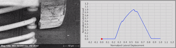
Figure 2. Miniaturizing lateral shear tests inside a scanning electron microscopy allows for quality control and failure mode investigations for novel wire bonding systems. Image Credit: Alemnis AG
Micromechanical Testing for Semiconductor Materials
SEM-based micromechanical testing is the key to unlocking quantitative mechanical properties of small volumes of materials.
The advantages this technique offers on the device- and components level also extends down to a materials level, whether single-crystalline structures, materials interfaces, or metallic patterns are being investigated.
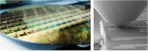
Figure 3. Across length scales: A full-scale wafer (left) in comparison to an individual pad being probed with a sharp diamond nanoindenter (right). Image Credit: Alemnis AG
Furthermore, the mechanical strength of microstructures in patterned semiconductor materials is strongly dependent on the fabrication techniques used. This sensitivity is due to the varying surface quality and potential ion implantation. The ability to measure such effects offers great potential to optimize the strength of such structures.
Correlating Micromechanical with Analytical Techniques
SEM-based micromechanical testing also offers a multitude of correlative approaches. In situ Raman spectroscopy, for example, is a well-established technique to evaluate stresses in semiconductor materials.
If combined with mechanical loading, this method can be exploited to obtain quantitative stress gradients during loading and residual stresses after loading.2
In situ EBSD measurements, on the other hand, allows for the measurement of elastic strain and stress tensors. Finally, digital image correlation techniques based on predeposited speckle patterns enable the evolution of total strain to be followed with nanoscale resolution.
Another exciting approach is to combine electrical microprobing while exerting mechanical stresses. Mechanical stress is known to change the band structure of materials. For example, mechanical stress can increase band-to-band tunneling of charge carriers in the overlap region between gate and drain.3
Understanding such leakage can be used to optimize device architecture and insure longer and safer operation.
Extreme Conditions Testing
Downsizing mechanical testing also facilitates investigations under extreme conditions, not least because of the vacuum environment inside an SEM. Extreme temperatures ranging from -150 °C up to 1000 °C can now routinely be attained.
The deformation and fracture behavior at elevated and cryogenic temperatures of semiconductor materials is of particular interest for the design of micro-electromechanical systems (MEMS). For example, most III–V semiconductor materials exhibit brittle-to-ductile transitions on increasing temperatures.
Understanding such fundamental behavior is an important objective, especially in view of its dependence on the nature of doping.1 Micromechanical testing at such conditions can help to map out operating temperature limits for a given minimum strength.
Furthermore, the mechanical properties of semiconductor materials can be extremely sensitive to changes in strain rates, which translates to impact or shock resistance in real-world applications.
For component design and lifetime prediction, it is thus important to also tabulate micromechanical properties under such non-ambient conditions.
High Throughput Characterization
Fast indentation mapping is an extremely useful technique for mapping mechanical properties across predefined areas of interest. The Alemnis Automated Large Sample Platform (ALSP) can accommodate wafers up to 4 inch in diameter, allowing any specific area of the wafer to be targeted.
The Alemnis Standard Assembly (ASA) is a fully automated test platform that is dedicated to measuring the mechanical properties of highly localized areas of a system, whether discrete or as part of a wafer containing many thousands of devices.
A wide choice of indenter geometries and test methods (indentation, scratch, tribology), coupled with SEM imaging, make this modular solution the ideal choice for in-line characterization.
The utilization of such an automated test platform on an IC production line allows for a fast and efficient way of probing mechanical properties in a highly reproducible manner and in conformance with up-to-date ISO and ASTM standards.
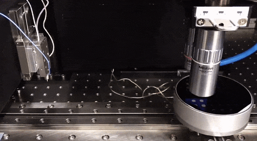
Figure 4. The Alemnis AG Automated Large Sample Platform can be used for a wide range of applications including semiconductor wafer mapping (e.g., bonding pads, MEMS structures, accelerometer beams, membranes, etc..), coatings with deposition gradients, and combinatorial material libraries. Image Credit: Alemnis AG

This information has been sourced, reviewed and adapted from materials provided by Alemnis AG.
For more information on this source, please visit Alemnis AG.