Multilayer dielectric stacks are used in various applications that demand accurate optical filtration, such as the military, aerospace, architectural glass, and all forms of optical metrology equipment, including Raman spectroscopy and 3D optical profilometry. These dielectric stacks precisely control the light’s reflection and transmission.

Image credits: Filmetrics, a KLA company
Individual high-pass (HP), low-pass (LP), and band-pass (BP) filters can be combined to make a highly specific filter by adjusting the thickness of the film layers. Typically, alternating layers of two to three materials produce the desired filter effect. The structure is called an “AB” stack when only two materials are used.
Measurement Setup
“How many layers can be measured?” is a frequently asked question. A variety of parameters influence this number. In this massive multilayer example, a Filmetrics system demonstration addressed a film stack, where the number of alternating layers and their materials were unknown.
While most measurements use 2-10 layer film stacks, the Filmetrics® FILMeasure® software algorithms can handle many more. The sample used was a commercially available dielectric stack on a fused silica substrate, as shown in Figure 1, with a scattering layer added to the bottom.
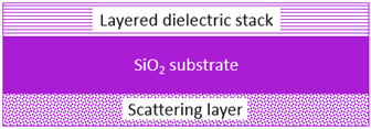
Figure 1. Rough schematic of the multilayer dielectric stack sample. Due to the presence of the back scattering layer, not much light was initially transmitted through the sample. Image Credit: Filmetrics, a KLA Company
Due to its wide spectral range of 190-1700 nm, the Filmetrics F10-RT-UVX Thin-Film Analyzer was selected to analyze the unknown total thickness film stack. For thick and complicated film stacks involving analysis with multiple variables, a wide wavelength range provides additional data required for determining a unique measurement solution.
Results and Discussion
Figure 2 shows the reflectance spectrum of the sample. The wavelength region between 400 nm and 620 nm was responsive to the thicknesses of the alternating layers. However, the wavelength region beyond 620 nm was sensitive to the overall stack thickness.
For alternating layer stacks such as this, the location and width of the reflectance response are determined by the ratio of layer A's average thickness to layer B's average thickness.
Figure 2 demonstrates near-100% reflectance in the 450 nm to 600 nm wavelength region, indicating that the film stack designer intended to create a highly reflective material in this range.
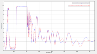
Figure 2. The sample’s reflectance spectrum (measured = blue, calculated = red), where the 400-620 nm wavelength range is sensitive to the alternating layer thicknesses, and > 620 nm is sensitive to the total thickness of the stack. Image Credit: Filmetrics, a KLA Company
In this example, only two materials were needed to represent the spectrum: the low-index material was SiO2, and the high-index material was presumably TiO2, Ta2O5, HfO2, or a comparable substance, based on materials generally used for these applications.
By altering the number of layers in the stack, it was discovered that more than 10 layers were needed to reflect the right side of the spectrum. Further modification was necessary to establish the specifics of the individual layers.
The FILMeasure® program provided a unique solution consisting of individual layers of varied thickness, with the mean SiO2 layer thickness measuring 107 nm, and the mean (unknown) high-index layer measuring 36 nm.
A piece of the scattering layer was removed to further investigate the stack, as demonstrated in the Figure 3 schematic and the Figure 4 image. This was carried out so that light could pass through the sample. With this layer eliminated, it was possible to acquire the transmission spectrum, illustrated in Figure 5.
The F10-RT-UVX concurrently gathers reflectance and transmittance spectra, and the FILMeasure spectral fitting is applied to both spectra to enhance the accuracy of the results. In this case, using both reflectance and transmittance data resulted in a better and physically accurate model. This is a significant advantage for these types of applications.
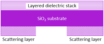
Figure 3. Schematic of the multilayer dielectric stack sample with a portion of the scattering layer removed to facilitate light transmission through the stack and substrate. Image Credit: Filmetrics, a KLA Company
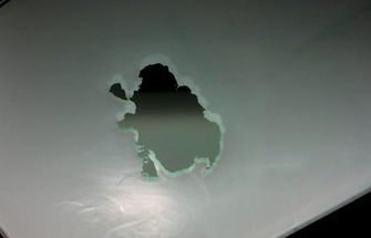
Figure 4. A close-up view of the video image from the F10-RT-UVX shows the removed area of the scattering layer. Image Credit: Filmetrics, a KLA Company
For the modeling methods, it must be emphasized that the algorithm did not produce multiple-thickness solutions (a real possibility when dealing with a high number of variable factors), and the final solution was unique. The overall goodness of fit (GOF) for the reflectance and transmittance spectra was > 0.99.
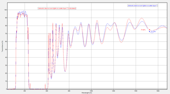
Figure 5. The sample’s transmission spectrum (measured = blue, calculated = red) simultaneously provides additional data for the FILMeasure model. Image Credit: Filmetrics, a KLA Company
According to Dr. Jim Elman, Filmetrics Applications Manager, "FILMeasure® and FILMapper provide a cost-effective thin film modeling solution used on thousands of instruments around the world. However, sitting under the hood are some powerful features that most users don’t encounter, which support the ability to handle an extremely complicated thin film stack.”
Conclusions
The Filmetrics F10-RT-UVX Thin-Film Analyzer with FILMeasure software successfully assessed a complex, unknown dielectric film stack, resolving not only the number of layers and the index of refraction of the high index substance but also the thickness of each of the 53 individual layers.
The initial question, “How many layers can be measured?”, has now been answered. The answer, in this case, is 53. With 53 individual layers measured, the customers of Filmetrics can measure 5, 10, 15, and more layers confidently.
About the Filmetrics F10-RT-UVX
The Filmetrics F10-RT Thin-Film Analyzer requires a mouse-click to capture reflectance and transmittance spectra by removing the requirement for hardware configuration changes between measurements.
The F10’s true normal incidence design is crucial for accurately characterizing display films. The video camera with image capture ensures easy and recordable measurement location. The industry-standard FILMeasure software brings the power of Filmetrics analysis to provide accurate analysis for several different types of applications.
Contact Filmetrics today to schedule thickness measurement on your thin film samples, or 3D surface topography using the Filmetrics Profilm3D® optical profiler, which quickly and easily analyzes surface roughness, step height, or other features of interest.

This information has been sourced, reviewed and adapted from materials provided by Filmetrics, a KLA Company.
For more information on this source, please visit Filmetrics, a KLA Company.