Sponsored by Nanosurf AGJan 12 2023Reviewed by Olivia Frost
Graphene is the most well-known member of the 2D materials family. It consists of a sheet of covalently bonded carbon atoms in a hexagonal lattice with the thickness of a single atom.
This unique nanomaterial is remarkably strong and has the highest thermal and electrical conductivity of any known material. Andre Geim and Konstantin Novoselov were awarded the Nobel Prize for Physics in 2010 for graphene research.
Several 2D materials other than graphene are also being actively explored. Xenes are a collective group of structures that resemble graphene and are likewise monolayers of a single element.
Phosphorene, a single layer of black phosphorus, is an attractive material for use in transistors. Other examples include silicene (silicon), germanene (germanium), and stanine (tin), all of which display a hexagonal structure with varying degrees of buckling, similar to graphene.
Hexagonal boron nitride (h-BN) has the same general structure as graphene but replaces the carbon atoms with boron and nitrogen atoms alternatively.
Transition metal dichalcogenides with the chemical formula MX2 are another popular class of 2D materials, where M is a transition metal such as tungsten or molybdenum and X is a chalcogen such as sulfur, selenium, or tellurium.
The stacking of graphene on itself or other 2D materials has recently gained increasing research interest. An angular or lattice mismatch results in the creation of a layered stack with unique electrical properties.
This paves the way for the production of new devices using a bottom-up approach by stacking multiple layers of 2D materials at angles that allow tuning of the properties. However, control measurements are necessary to verify the angular mismatch between the layers since relaxation processes occur after deposition.
Why AFM?
AFM has become the tool of choice for researching nanomaterials for two major reasons: resolution and the many different modes that are available to comprehensively characterize a nanomaterial, including its mechanical and electrical properties beyond the topography. The remarkable x-, y-, and z-resolution are important due to atomic-scale phenomena.
A commercial AFM’s resolution varies from a few nanometers to atomic resolution laterally and greater than 0.1 nm vertically. As a result, AFM is one of the few instruments capable of attaining the resolution required for the measurement of nanosheets as thin as a few angstroms.
Another real-world benefit of AFM is the accessible array of measurement modes for simultaneously detecting electrical and mechanical properties to the topography.
These modes can be used for in-depth investigation of those additional properties or simply as a contrast mechanism to assess the quality of grown graphene or the angular mismatch between stacked layers. This makes AFM a very useful instrument for device design that relies on the stacking of 2D materials.
The AFM tip can also be used to manipulate nanoscale samples. In the case of graphene, it can be used to cut through graphene sheets. The two sides of a single graphene sheet cut in two have the same crystal orientation, improving the control of the angular mismatch during stacking.
Aside from imaging capabilities, another reason for using AFM is its compact footprint, which allows it to be placed inside a glovebox. This is great when it comes to studying graphene in combination with 2D materials that are sensitive to the presence of oxygen or humidity.
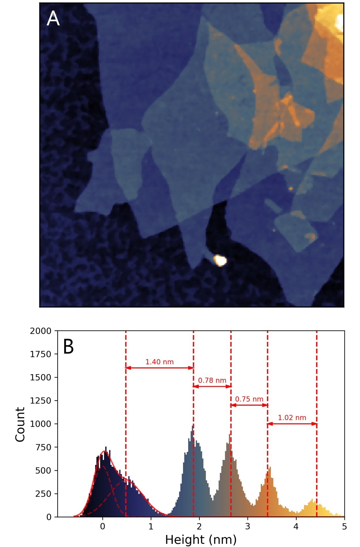
Figure 1. Measuring the thickness of multilayer graphene. (A) AFM topographical image of graphene oxide with lateral dimensions of 5.11 x 5.11 µm2. (B) Histogram of the heights in (A) showing the thickness of the first 4 layers. Sample courtesy: Nanotech Energy, USA.
Applications
The following applications demonstrate the ability of AFM to characterize graphene.
1. Flake Thickness
The first example demonstrates the remarkable resolution of AFM. Figure 1 depicts several stacked layers of graphene oxide, allowing for the thicknesses of the individual layers to be calculated.
A corresponding height histogram of the measurement demonstrates that the thinnest layer is only 0.75 nm thick. This image demonstrates AFM’s exceptional vertical resolution at the level necessary for studying 2D materials.
2. Graphene Growth Analysis
Figure 2 is an illustration of the AFM’s ability to examine the quality of graphene. The sample consists of graphene grown on copper using a chemical vapor deposition (CVD) process. The copper substrate is not atomically flat, which can obscure the edges and fine features of the flakes.
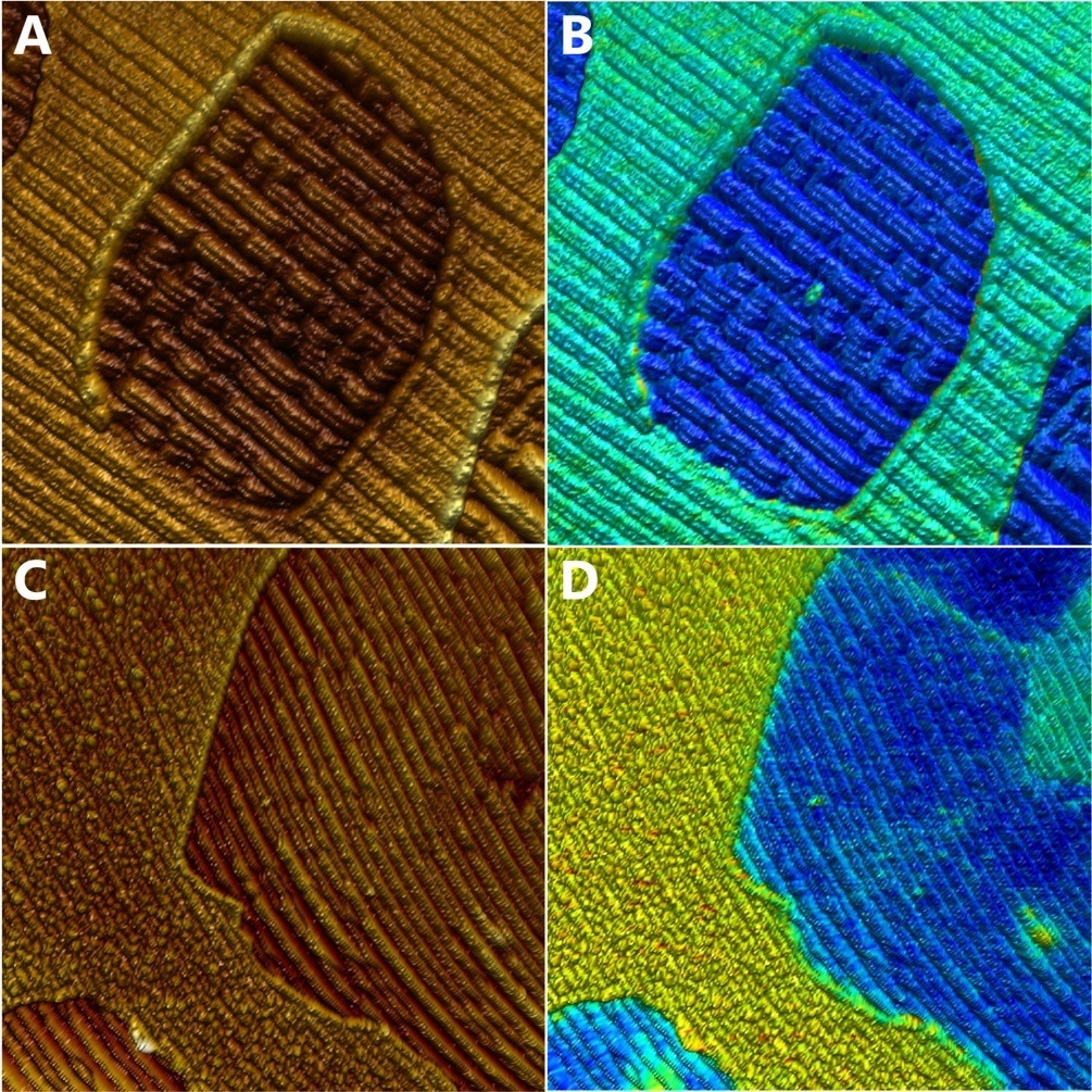
Figure 2. Quality control of chemical vapor deposition (CVD) grown graphene on post-oxidized copper by lateral force imaging and KPFM. (A) Topography and (B) friction force images, simultaneously recorded. The friction was calculated from the difference between the forward and backward lateral deflection channels. Scan size: 5 x 5 µm2. (C) Topography and (D) contact potential difference images. Scan size 10 x 10 µm2. Data courtesy: Newtec, A/S Denmark.
The copper was oxidized after the deposition, causing the height of the oxidized copper to exceed that of the graphene flake in the topography (Figures 2A and 2C). The lateral force image (Figure 2B) reveals lower friction on the graphene (blue contrast) compared to the copper substrate (green contrast).
This facilitates the analysis of the graphene coverage of the copper substrate, as edges have a more pronounced contrast in the friction channel than in the topography. Moreover, the friction image demonstrates higher friction in the center of the flake, highlighting the flake’s growth seed point that is not visible in the topography.
The sample was also analyzed by using a Kelvin probe force microscope (KPFM) (Figure 2D). Traditionally, KPFM is used to examine the contact potential difference (CPD) between tip and sample and even the work function under a vacuum setting.
As anticipated, graphene and oxidized copper have distinct CPD values, with graphene having a lower value. The CPD image also reveals heterogeneity in the graphene, with some small lines and sites on the graphene flakes that are not recognizable in the topography, thus improving the AFM’s ability to evaluate the quality assessment of the graphene deposition process.
3. Lattice Mismatch
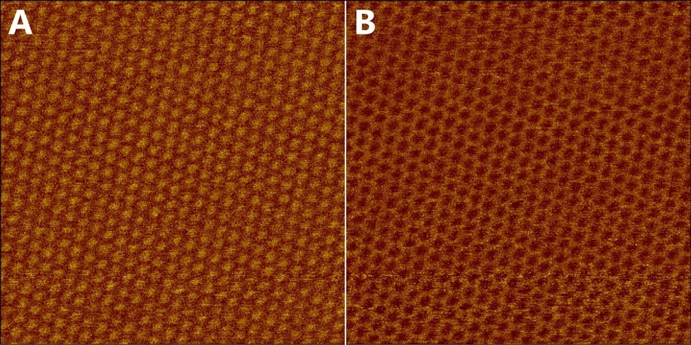
Figure 3. Moiré super lattice of twisted graphene on hBN imaged in PFM mode at the contact resonance frequency. (A) amplitude and (B) phase. Scan size: 154 x 154 nm2. Sample courtesy: Nanoelectronics group TIFR, India.
The interface between the AFM tip and a graphene layer also depends on the graphene layer’s interaction with the layer underneath it. In the case of an angular mismatch, the interaction fluctuates regularly with a lattice constant that changes according to the angular mismatch.
This regular pattern, also called moiré super lattice, may be observed using AFM, for example, via piezo-response force microscopy (PFM)1 or force modulation,2 swinging the cantilever at the contact resonance frequency. A cantilever with its tip in contact with the sample has different resonances than a free-swinging cantilever.
The initial contact resonance is very sensitive to the sample’s mechanical characteristics. The contact resonance can be detected directly with a phase-locked loop or dual frequency resonance tracking or indirectly by detecting the phase and amplitude of the cantilever triggered at a fixed frequency during the contact resonance peak.
This contact resonance frequency can be found by analyzing a thermal tune spectrum captured with the tip in contact with the sample. From the periodicity of the moiré superlattice, the angular mismatch between two layers of graphene can also be determined.
Figure 3 demonstrates the phase and amplitude response produced by imaging a double layer of twisted graphene, depicting the moiré pattern caused resulting from an angular mismatch.
The cantilever was electro-statically triggered in PFM mode at the contact resonance frequency. The angular mismatch of this sample was determined to be 2.2° based on the lattice constant of the moiré pattern.
Figure 4 shows the phase response observed in the force modulation imaging mode of a DriveAFM instrument.2 In this case, the cantilever was photothermally stimulated at the contact resonance peak.
The 192 nm wide image of Figure 4A depicts a lattice with some distortion, suggesting a fluctuation in the angular mismatch but still yielding multiple diffraction spots in frequency space after Fourier transformation (Figure 4B).
The frequency of 1/(7.26 nm) of the (2;2) diffraction spot adjacent to the fast scan axis translates to a lattice constant of 29 nm in real space.
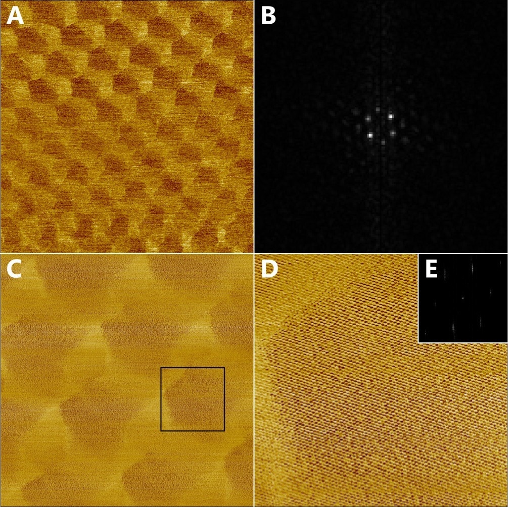
Figure 4. Moiré super lattice of twisted graphene on hBN imaged in force modulation mode on the contact resonance frequency. (A) phase image with scan size of: 190 x 190 nm2 (B) Center part of the Fourier transform image used to determine the lattice constant of the moiré pattern (C) phase image of 68 x 68 nm2 area rescanned with 1024 x 1024 px2 containing both the moiré superlattice and atomic lattice. (D) Digital zoom of the (C). (E) Fourier transform showing the diffraction spots from the atomic lattice. Sample courtesy: Nanoelectronics group TIFR, India.
This is 117 times greater than graphene’s lattice constant, demonstrating an angular mismatch close to 0.5°. A 68 nm wide image (C) recorded with 1024 x 1024 px2 shows not only the moiré superlattice but also the atomic lattice.
Figure 4D displays a digital zoom of 17 nm in phase signal width to improve visualization of the lattice in real space, and Figure 4F demonstrates the Fourier transform of the phase signal. The moiré super lattice’s lattice was verified using the atomic lattice.
4. Cutting Graphene
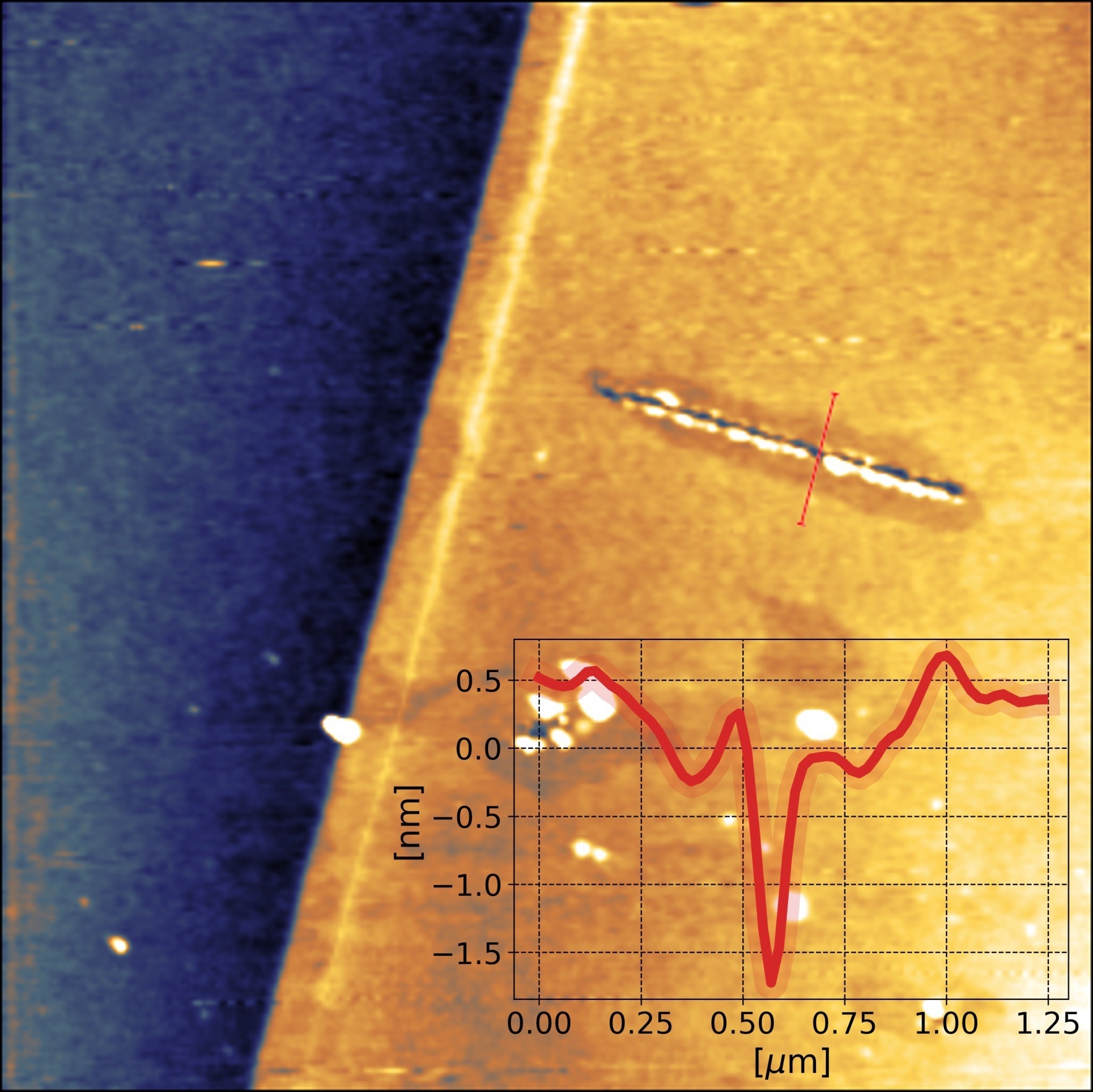
Figure 5. Cutting graphene by AFM lithography. AFM topography image of a multilayer graphene flake on Si substrate with lateral dimensions of 10 x 10 µm2. Cuts were obtained by applying a 10V AC voltage at 500 kHz to the tip of a BudgetSensors ElectriTap190E cantilever (k = 48 N/m nominal) and following the designated path in Static Force Mode with an applied force of 5 µN at a speed of 100 nm/s. The relative humidity was 42%. Sample courtesy: Kim group, Harvard University, USA.
The AFM tip can be used to not only measure but also manipulate materials on the nanometer scale. Figure 5 depicts a multi-layer stack of graphene cut with an AFM tip in nanolithography mode. The experiment was performed on a FlexAFM.
Several parameters, such as force, speed, and direction, may be used to regulate cutting in lithography. A DC or AC voltage, or a combination of both, can be applied between tip and sample at the same time to influence the depth of the cut. It is believed that the cutting mechanism occurs via local anodic oxidation of the surface.3-5
The high voltages near the tip split H2O into H and OH groups, oxidizing the graphene. The tip-induced mechanical stress subsequently fractures the graphene at the oxidized locations. This is why the relative humidity around the tip is so important in graphene cutting. The environmental control add-on enables precise humidity control around samples.
Conclusion
Graphene and other 2D materials like xenes (or transition metal dichalcogenides) are a fast-growing topic of interest among leading nanomaterials researchers, with intriguing applications in transistors, sensors, and optoelectronics.
AFM is ideally suited to examine such materials because of its impressive resolution, well below a nanometer, capable of clearly showing the atomic lattice and atomic steps.
AFM can measure and correlate numerous critical aspects of these materials as a multifunctional characterization method, allowing us to better understand and characterize them. One example of this type of characterization is the identification of moiré patterns. In addition, AFM can also be used to locally manipulate 2D materials.
In conclusion, AFM is an indispensable tool for studying graphene and other 2D materials for eventual integration into devices and other applications.
References
- McGilly et al 2020 Nat. Nanotechnol. 15, 580– 584
- Adams et al 2021 Rev. Sci. Instr. 92, 129503
- Puddy et al 2011, Appl. Phys. Lett. 98, 133120
- Masubuchi et al 2011, Nano Lett. 11, 4542–4546
- Li et al 2018, Nano Lett. 18, 8011-8015

This information has been sourced, reviewed and adapted from materials provided by Nanosurf AG.
For more information on this source, please visit Nanosurf AG.