Sponsored by Nanosurf AGJan 5 2023Reviewed by Olivia Frost
Graphene is the most prominent member of the 2D materials family: just a single atom in thickness, it is a sheet of covalently bonded carbon atoms in a hexagonal lattice. This novel nanomaterial is exceptionally strong and has the greatest known thermal and electrical conductivity. Andre Geim and Konstantin Novoselov received the Nobel prize for Physics in 2010 for their research in relation to this wonder material.
Today, researchers are exploring numerous other 2D materials. A collective group of graphene-like structures, known as xenes, are monolayers of a single element. For instance, a single layer of black phosphorus, phosphorene, is a likely candidate material for transistors.
Other examples are germanene (germanium), silicene (silicon), and stanine (tin), all exhibiting a graphene-like hexagonal structure with various degrees of buckling. Hexagonal boron nitride (h-BN) has the same general structure as graphene, but the carbon atoms are substituted for alternating boron and nitrogen atoms.
Finally, other members of a popular class of 2D materials are transition metal dichalcogenides with the chemical formula MX2, where M represents a transition metal, such as tungsten or molybdenum, and X represents a chalcogen, such as sulfur, selenium, or tellurium.
There is increased interest in stacking graphene or other 2D materials. An angular or lattice mismatch of the layered stack has been shown to produce various electrical properties and outcomes.
This paves the way to constructing new devices in a bottom-up approach, stacking several layers of 2D materials under such angles to tune the properties. However, control measurements are necessary to quantify the angular mismatch between the layers as relaxation processes after deposition occur.
Why AFM?
AFM is now the instrument of choice for studying nanomaterials for two main reasons: resolution and availability of several different modes facilitating detailed characterization of a nanomaterial, including its mechanical and electrical properties beyond the topography. Achieving excellent x-, y-, and z resolution are crucial when evaluating phenomena close to the atomic scale.
AFM is one of the few instruments that can achieve the requisite resolution to measure nanosheets that are only a few angstroms thick. This is down to the resolution of a commercial AFM ranging from less than a few nanometers to atomic resolution laterally, and better than 0.1 nm vertically.
Another benefit that AFM offers with real-world implications is the available suite of measurement modes to evaluate electrical and mechanical properties simultaneously with the topography. These modes can be applied to study additional properties in detail, or simply as a contrast mechanism to determine the quality of grown graphene or the angular mismatch between stacked graphene layers.
This makes AFM an essential tool for device design dependent on the stacking of 2D materials. Moreover, the AFM tip can be applied to manipulate samples at the nanoscale. Concerning graphene, it can, for instance, be used to slice through graphene sheets. The two halves of a single graphene sheet cut in two possess the same crystal orientation, improving control over the angular mismatch during stacking.
In addition to these imaging properties, another motivation for using AFM stems from its small footprint, allowing it to be placed inside a glovebox. This is a prerequisite when studying graphene in combination with 2D materials that are vulnerable to the presence of oxygen or humidity.
Applications
Examples of the power of AFM to characterize graphene are described in each of the following applications:
1. Flake thickness: The first example demonstrates the excellent quality of AFM resolution. Figure 1 shows several stacked layers of graphene oxide, facilitating analysis of the thicknesses of the individual layers. The thinnest layer is a mere 0.75 nm as displayed in the corresponding height histogram of the measurement. This image exhibits the excellent vertical resolution that AFM delivers at the level required to study 2D materials.
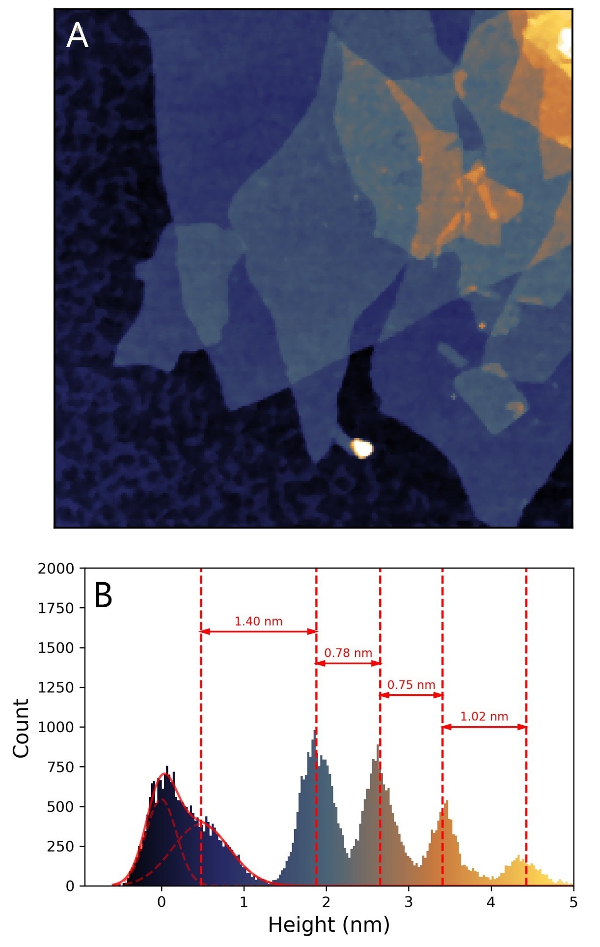
Figure 1. Measuring the thickness of multilayer graphene. (A) AFM topographical image of graphene oxide with lateral dimensions of 5.11 x 5.11 μm2. (B) Histogram of the heights in (A) showing the thickness of the first 4 layers. Sample courtesy: Nanotech Energy, USA. Image Credit: Nanosurf AG
2. Graphene growth analysis: An example of the capability to verify the quality of graphene is displayed in Figure 2. The sample is comprised of graphene grown on copper by chemical vapor deposition (CVD). The copper substrate is not atomically flat, sometimes concealing the edges and fine features of the flakes. Post-deposition, the copper was oxidized, which resulted in the height of the oxidized copper surpassing that of the graphene flake in the topography (Figure 2A and 2C).
The lateral force image (Figure 2B) displays lower friction on the graphene (blue contrast) in contrast to the copper substrate (green contrast) which supports graphene coverage analysis of the copper substrate, since edges exhibit a sharper contrast in the friction channel than in the topography.
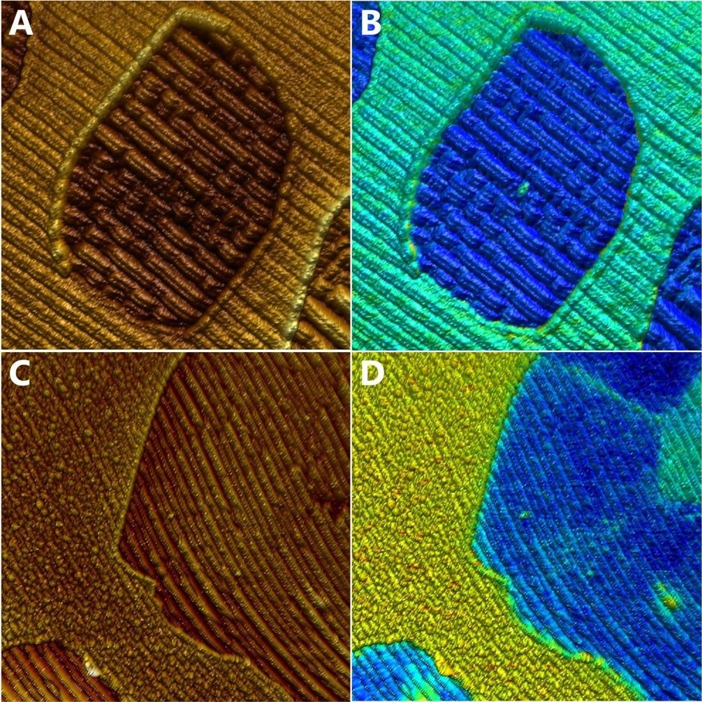
Figure 2. Quality control of chemical vapor deposition (CVD) grown graphene on post-oxidized copper by lateral force imaging and KPFM. (A) Topography and (B) friction force images, simultaneously recorded. The friction was calculated from the difference between the forward and backward lateral deflection channels. Scan size: 5 x 5 μm2. (C) Topography and (D) contact potential difference images. Scan size 10 x 10 μm2. Data courtesy: Newtec, A/S Denmark. Image Credit: Nanosurf AG
The friction image demonstrates a greater rate of friction in the center of the flake, determining the growth seed point of the flake that is not visible in the topography. Kelvin probe force microscopy (KPFM) was also applied to the analysis of this sample (Figure 2D).
KPFM is traditionally used to analyze the contact potential difference (CPD) between tip and sample, and under vacuum conditions even the work function. As anticipated, graphene and the oxidized copper demonstrate a difference in CPD, with graphene possessing a lower value. Crucially, the CPD image exhibits a heterogeneity on the graphene, with some fine lines and areas on the graphene flakes that are not discernable in the topography, improving the quality assessment of the graphene deposition process using AFM.
3. Lattice mismatch: The interaction between the AFM tip and a graphene layer is contingent on the interaction of the graphene layer with the underlying layer. When an angular mismatch is present, the interaction periodically varies with a lattice constant depending on the angular mismatch. This basic pattern, also known as moiré super lattice, can be visualized with the application of AFM, for instance by piezo-response force microscopy (PFM)1 or force modulation2, oscillating the cantilever at the contact resonance frequency.
A cantilever with the tip in contact with the sample has various resonances compared to a free-swinging cantilever. The first contact resonance is extremely sensitive to the mechanical properties of the sample. The contact resonance can be measured with a phase-locked loop or dual frequency resonance tracking directly or indirectly and is much simpler by identifying the phase and amplitude of the cantilever excited at a fixed frequency on the contact resonance peak.
This contact resonance frequency can be established using a thermal tune spectrum recorded with the tip in contact with the sample. Applying interpretation of the periodicity of the moiré superlattice facilitates calculations of angular mismatch between two layers of graphene.
Figure 3 displays the phase and amplitude response acquired by imaging a double layer of twisted graphene, clearly indicating the moiré pattern that appears as a result of an angular mismatch. The cantilever was electro-statically excited in PFM mode at the contact resonance frequency. The angular mismatch of this sample amounted to 2.2° as based on the lattice constant of the moiré pattern.
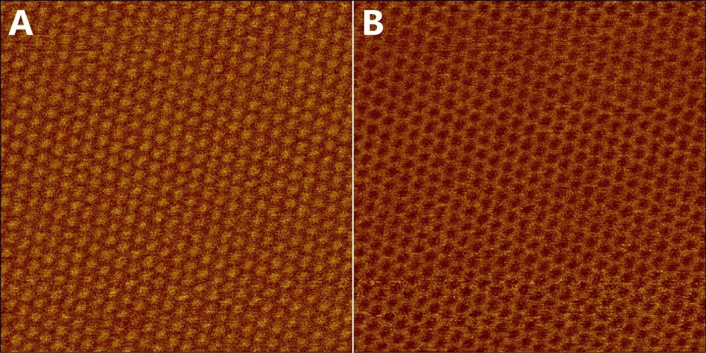
Figure 3. Moiré super lattice of twisted graphene on hBN imaged in PFM mode at the contact resonance frequency. (A) amplitude and (B) phase. Scan size: 154 x 154 nm2. Sample courtesy: Nanoelectronics group TIFR, India. Image Credit: Nanosurf AG
Figure 4 demonstrates how the phase response was measured in force modulation imaging mode on a DriveAFM2. Here, the cantilever was photothermally excited on the contact resonance peak. The 192 nm wide image of Figure 4A exhibits a lattice with slight distortion, suggesting a variation in the angular mismatch, but still offering multiple diffraction spots in frequency space after Fourier transformation (Figure 4B).
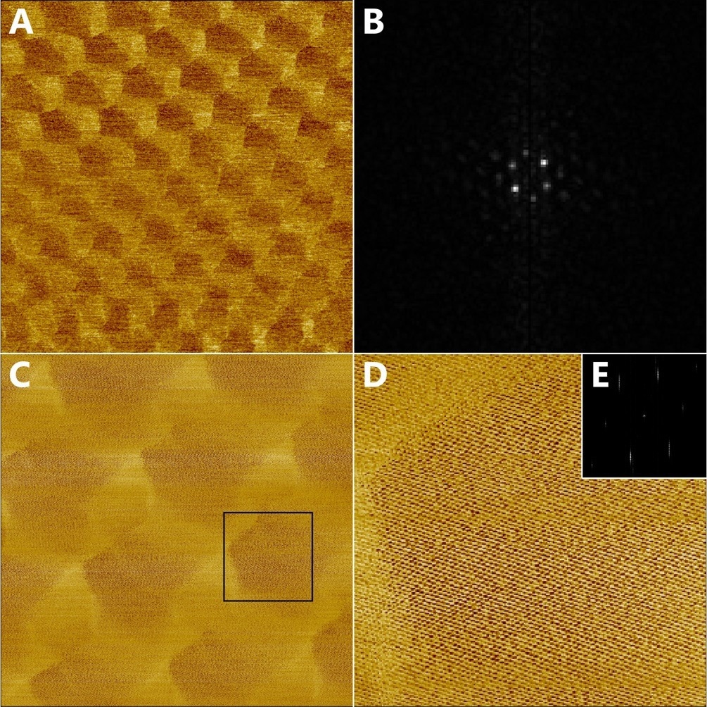
Figure 4. Moiré super lattice of twisted graphene on hBN imaged in force modulation mode on the contact resonance frequency. (A) phase image with scan size of: 190 x 190 nm2 (B) Center part of the Fourier transform image used to determine the lattice constant of the moiré pattern (C) phase image of 68 x 68 nm2 area rescanned with 1024 x 1024 px2 containing both the moiré superlattice and atomic lattice. (D) Digital zoom of the (C). (E) Fourier transform showing the diffraction spots from the atomic lattice. Sample courtesy: Nanoelectronics group TIFR, India. Image Credit: Nanosurf AG
The frequency of 1/(7.26 nm) of the (2;2) diffraction spot near the fast scan axis switches to a lattice constant of 29 nm in real space. This is 117 times greater than the lattice constant of graphene, demonstrating an angular mismatch close to 0.5°. Recording a 68 nm-wide image (C) with 1024 x 1024 px2 not only shows the moiré superlattice but also reveals the atomic lattice.
A digital zoom of 17 nm in width of the phase signal is displayed in Figure 4D, to improve the visibility of the lattice in real space. Figure 4F exhibits the Fourier transform of the phase signal. The atomic lattice was utilized to validate the lattice of the moiré superlattice.
4. Cutting graphene: As previously mentioned, the AFM tip can be utilized to measure and manipulate materials on the nanometer scale. An example of a multi-layer stack of graphene sliced with an AFM tip in nanolithography mode is displayed in Figure 5.
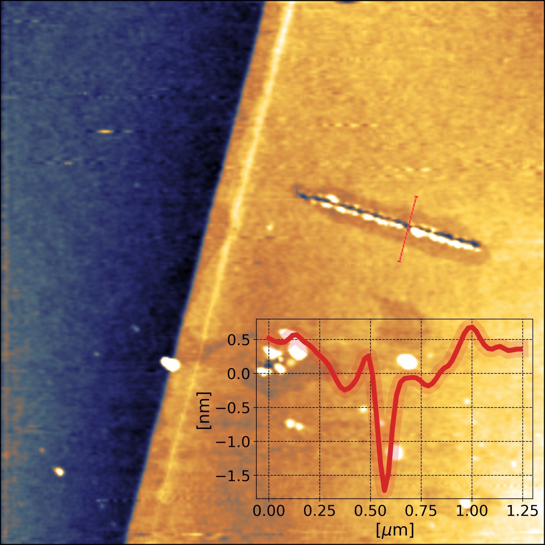
Figure 5. Cutting graphene by AFM lithography. AFM topography image of a multilayer graphene flake on Si substrate with lateral dimensions of 10 x 10 μm2. Cuts were obtained by applying a 10V AC voltage at 500 kHz to the tip of a BudgetSensors ElectriTap190E cantilever (k = 48 N/m nominal) and following the designated path in Static Force Mode with an applied force of 5 μN at a speed of 100 nm/s. The relative humidity was 42%. Sample courtesy: Kim group, Harvard University, USA. Image Credit: Nanosurf AG
The experiment was conducted on a FlexAFM. In lithography, cutting can be manipulated by controlling several parameters, such as force, speed, and direction.
At the same time, applying a DC or AC voltage, or a combination of both, between tip and sample can help influence the depth of the cut. It is believed that the cutting mechanism is present via local anodic oxidation of the surface.3-5 The high voltages close to the tip dissociate H2O into H and OH groups, which oxidize the graphene.
At the locations it was oxidized, the tip-induced mechanical stress fractures the graphene. This is why the relative humidity surrounding the tip plays a crucial role in graphene cutting. The environmental control add-on facilitates close control of the humidity surrounding samples.
Conclusion
Interest in graphene and other 2D materials such as xenes – or transition metal dichalcogenides – is picking up pace among leading nanomaterials researchers, with innovative applications in transistors, sensors, and optoelectronics.
AFM is well-suited to study such materials thanks to its exceptional resolution well below a nanometer, with the ability to indicate the atomic lattice and steps.
As a multifunctional characterization tool, AFM can measure and correlate several critical properties of these materials to improve understanding and enhance characterization.
The ability to detect moiré patterns is one such example of this type of characterization. AFM can also be applied to manipulate 2D materials locally. This makes AFM an essential tool when studying graphene and other 2D materials in search of ultimate integration into devices and alternative applications.
References and Further Reading
- McGilly et al. 2020 Nat. Nanotechnol. 15, 580– 584
- Adams et al. 2021 Rev. Sci. Instr. 92, 129503
- Puddy et al. 2011, Appl. Phys. Lett. 98, 133120
- Masubuchi et al. 2011, Nano Lett. 11, 4542–4546
- Li et al. 2018, Nano Lett. 18, 8011-8015

This information has been sourced, reviewed and adapted from materials provided by Nanosurf AG.
For more information on this source, please visit Nanosurf AG.