Applied Materials, Inc. today announced that its Applied SEMVision™ G4 Defect Analysis platform has been honored with the prestigious Editors' Choice Best Product Award by Semiconductor International (SI) magazine. The winning combination of innovative technology and production-proven performance has made the SEMVision G4 platform the defect review tool of choice for 32nm design rules and beyond.
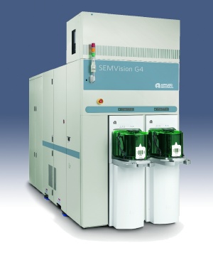 Innovative technology and production-proven performance have made the Applied SEMVision G4 platform the defect review tool of choice for 32nm design rules and beyond. (Photo: Business Wire)
"The Editors' Choice Best Products awards program acknowledges products, materials and services that are proven in the manufacturing environment," said Laura Peters, Editor-in-Chief of Semiconductor International. “In the evaluation process, SI's editors consider the products based on feedback from actual customers in the field and only the most highly recommended ones are honored each year.”
“This award recognizes the tremendous impact Applied’s SEMVision technology has had on the semiconductor industry,” said Tom St. Dennis, senior vice president and general manager of Applied Materials’ Silicon Systems Group. “The SEMVision G4 system’s exceptional image quality and advanced material analysis capabilities are powerful tools to help chipmakers understand and mitigate the root causes of yield-killing defects.”
The Applied Defect Review SEMVision systems are designed for the most advanced review applications, capable of automatic defect redetection (ADR) and automatic defect classification (ADC) of critical defects. Key features of the SEMVision G4 technology are its new scanning electron microscope (SEM) column and enhanced multi-perspective SEM imaging system that deliver state-of-the-art 2nm physical resolution for unmatched image quality at a benchmark review rate of one defect-per-second.
The Applied SEMVision system pioneered automatic defect review in 1998, revolutionizing the way fabs detect and analyze defect information. For the past ten years, SEMVision technology has provided enabling capability to the industry, with over 700 systems installed at customer sites worldwide. This is the third SI award for Applied’s SEMVision technology, beginning with the first SEMVision system in 2000 and continuing with the SEMVision G2 FIB in 2005.
Applied Materials, Inc. (Nasdaq:AMAT) is the global leader in Nanomanufacturing Technology™ solutions with a broad portfolio of innovative equipment, service and software products for the fabrication of semiconductor chips, flat panel displays, solar photovoltaic cells, flexible electronics and energy efficient glass. At Applied Materials, we apply Nanomanufacturing Technology to improve the way people live.